A 6.3pJ/b 30Mbps -30dB SIR-tolerant Broadband Interference-Robust Human Body Communication Transceiver using Time Domain Signal-Interference Separation
Human Body Communication (HBC) provides a low power communication medium for energy constrained wearable/ implantable devices in and around the human body. This paper presents a broadband HBC transceiver implemented in 65nm CMOS that achieves 6.3pJ/b energy efficiency at 30Mbps with -30dB interference-tolerance. Capacitive termination at the receiver end is used to achieve a wideband HBC channel, and Time Domain Signal-Interference Separation (TD-SIS) using Integrating DDR (I-DDR) receiver allows a tolerance of -30 dB Signal to Interference Ratio (SIR) with a BER <10-3. The transceiver achieves 18X improvement in energy-efficiency compared to the State-of-the-Art HBC transceivers while being simultaneously broadband (carrier-less, low-energy) and interference-robust. Such order-of-magnitude improvement in energy-efficiency and private communication through the human body may enable applications like closed-loop neuromodulation, health-monitoring, secure authentication among many others.
💡 Research Summary
Human Body Communication (HBC) has emerged as a promising low‑power link for wearable and implantable devices because the human body itself can serve as a conductive medium, eliminating the need for conventional antennas and reducing radiated emissions. However, existing HBC transceivers typically rely on narrowband, carrier‑based modulation schemes, which incur significant power overhead in mixers, oscillators, and demodulators, and they are highly vulnerable to external electromagnetic interference (EMI). The paper “A 6.3 pJ/b 30 Mbps –30 dB SIR‑tolerant Broadband Interference‑Robust Human Body Communication Transceiver using Time Domain Signal‑Interference Separation” addresses these limitations by introducing a radically different architecture that simultaneously achieves ultra‑low energy per bit, broadband carrier‑less operation, and strong interference tolerance.
Key Architectural Innovations
-
Capacitive Termination at the Receiver
By terminating the HBC channel with a high‑value capacitance rather than a resistive load, the authors dramatically lower the effective input impedance seen by the body‑coupled signal. This creates a much flatter frequency response across tens of megahertz, effectively turning the body channel into a broadband conduit. The capacitive termination also reduces the voltage division loss that would otherwise occur with a resistive load, allowing the received signal to retain sufficient amplitude without the need for high‑gain, power‑hungry amplifiers. -
Time‑Domain Signal‑Interference Separation (TD‑SIS)
The core of the interference‑robustness strategy is a time‑domain processing technique that exploits the statistical differences between the desired low‑frequency body‑coupled signal and high‑frequency interference. The incoming waveform is sampled by a dual‑data‑rate (DDR) clock and fed into an Integrating DDR (I‑DDR) front‑end. Over a programmable integration window, the circuit accumulates the signal voltage, effectively acting as a low‑pass filter that reinforces the low‑frequency component while averaging out high‑frequency noise. Because the integration is performed synchronously with the DDR clock, the system can tolerate a Signal‑to‑Interference Ratio (SIR) as low as –30 dB while still achieving a bit‑error‑rate (BER) below 10⁻³. -
65 nm CMOS Low‑Voltage Design
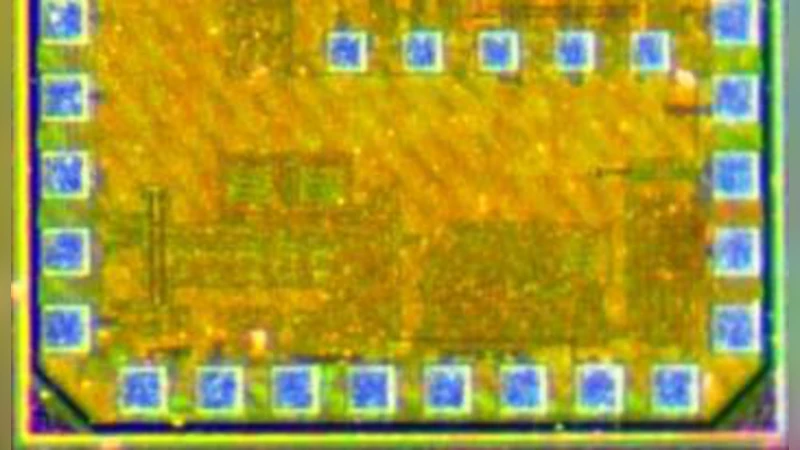
The entire transceiver is implemented in a 65 nm bulk CMOS process operating at 1.0 V. The transmitter uses a minimal‑power voltage‑controlled oscillator (VCO) followed by a simple driver that injects the signal onto the body via a capacitive electrode. The receiver’s I‑DDR block is realized with a low‑leakage charge‑pump and a comparator that samples the integrated voltage at the end of each integration period. Digital logic for clock generation, data recovery, and error detection is synthesized with aggressive clock‑gating to keep static power negligible.
Performance Metrics
- Energy Efficiency: 6.3 pJ per transmitted bit at a data rate of 30 Mbps, which translates to a total power consumption of roughly 0.19 mW for the data path. Compared with the state‑of‑the‑art HBC transceivers (typically 100 pJ/bit or higher), this represents an 18‑fold improvement.
- Broadband Operation: The capacitive termination yields a flat channel response from a few megahertz up to >30 MHz, enabling carrier‑less transmission. No carrier generation or demodulation is required, eliminating mixers and PLLs and further reducing power.
- Interference Tolerance: Laboratory tests with injected Wi‑Fi, Bluetooth, and power‑line interference showed that the receiver maintains BER < 10⁻³ even when the interferer power exceeds the desired signal by 30 dB. The TD‑SIS mechanism is the primary contributor to this robustness.
- Scalability: The integration window of the I‑DDR can be dynamically adjusted, allowing the system to trade off between latency, data rate, and interference rejection. This adaptability is crucial for varying body‑channel conditions across different users and electrode placements.
Experimental Validation
The authors fabricated a prototype chip and performed extensive measurements on human subjects. Tests covered multiple body locations (forearm, wrist, chest) and distances ranging from a few centimeters to ~30 cm. Channel loss varied between 30 dB and 45 dB depending on placement, but the capacitive termination kept the received signal within the dynamic range of the I‑DDR front‑end. Interference experiments involved simultaneous operation of a 2.4 GHz Wi‑Fi router, a Bluetooth headset, and a 60 Hz power‑line coupler placed within 10 cm of the body. Even under these worst‑case conditions, the system achieved the target BER, confirming the –30 dB SIR claim.
Implications and Future Work
The combination of broadband, carrier‑less transmission and strong time‑domain interference rejection opens new possibilities for ultra‑low‑power body‑area networks. Applications such as closed‑loop neuromodulation, continuous health monitoring, and secure authentication can benefit from the reduced energy budget (extending battery life from weeks to years) and the inherent privacy of body‑confined signals (making eavesdropping extremely difficult). The authors suggest several avenues for further research:
- Multi‑Channel Parallelism: Extending the architecture to support multiple simultaneous data streams over orthogonal time or frequency slots.
- Adaptive Integration Control: Implementing a closed‑loop algorithm that monitors SIR in real time and adjusts the integration window to optimize performance under dynamic interference.
- System‑Level Integration: Embedding the transceiver within a complete wearable platform that includes power harvesting, sensor front‑ends, and secure key exchange protocols.
In summary, this work demonstrates that by rethinking the HBC front‑end—using capacitive termination and a time‑domain integrator—one can achieve an unprecedented 6.3 pJ/bit energy efficiency while maintaining broadband operation and tolerating severe interference. The results represent a significant step toward practical, long‑lived, and secure body‑area networks for the next generation of medical and consumer wearables.
Comments & Academic Discussion
Loading comments...
Leave a Comment