Narrowband Bandpass Frequency Selective Surface with Miniaturized Elements
This article presents a bandpass frequency selective surface (FSS) with a narrowband frequency response. The designed FSS is made of miniaturized elements unit cell. The operation principle of the FSS is explained by using an equivalent circuit model…
Authors: Amir Ebrahimi, Thomas Baum, James Scott
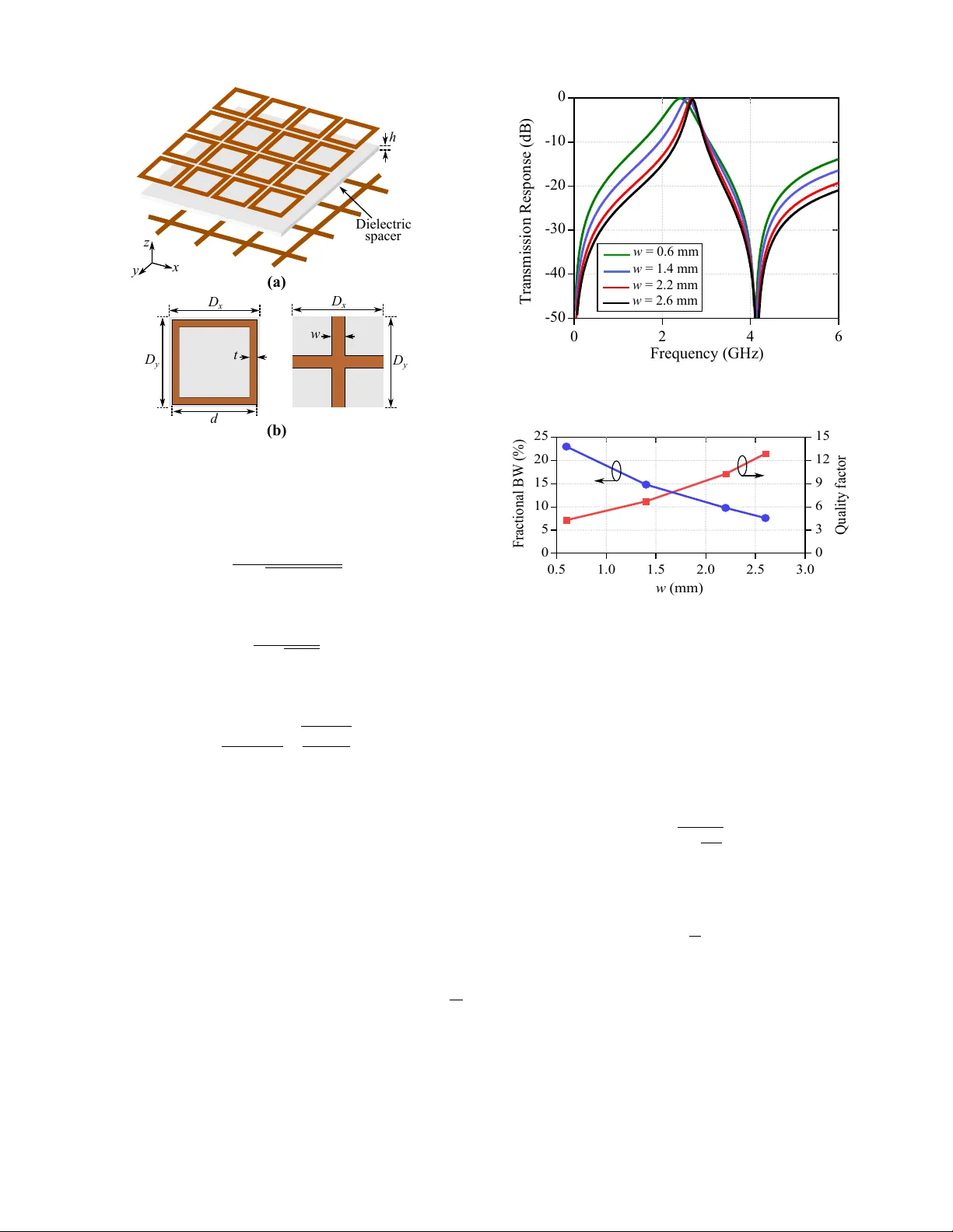
1 Narro wband Bandpass Frequenc y Selecti ve Surf ace with Miniaturized Elements Amir Ebrahimi, Member , IEEE, Thomas Baum Member , IEEE, James Scott Member , IEEE, and Kamran Ghorbani Member , IEEE, School of Engineering , Royal Melbourne Institute of T echnology (RMIT University), VIC 3001, A ustralia amir .ebrahimi@rmit.edu.au Abstract —This article presents a bandpass frequency selective surface (FSS) with a narro wband frequency r esponse. The designed FSS is made of miniaturized elements unit cell. The operation principle of the FSS is explained by using an equivalent circuit model, wher e the passband band width can be contr olled by the values of the cir cuit elements corresponding to the geometrical dimensions of the unit cell. The compatibility of the presented structure in designing higher order narrowband filter - ing responses is verified by designing a second-order bandpass FSS with 8 . 5% fractional bandwidth with a center frequency of 2 . 7 GHz. Index T erms —Frequency Selective Surfaces (FSSs), narrow- band filters, spatial filters. I . I N T RO D U C T I O N Frequency selecti ve surfaces (FSSs) are artificial periodic structures that can mani pulate the propagation of the elec- tromagnetic wav es by controlling their amplitude, phase, or polarization [1]. Due to their versatile functionalities, the FSSs hav e found a wide range of applications from low microwa ve to terahertz and optical frequencies [2]. F or example, the y can be designed as absorbers [3], reflect arrays [4], transmit arrays [5], polarization con vertors [6], [7], and etc. A major application of the FSSs is in spatial filtering of the electromag- netic radiations for reducing the radar cross-section (RCS) of the objects in stealth platforms, reducing the interferences in communications, and shielding the electronic devices against unwanted signals [1]. V ariety of the FSS-based filtering struc- tures have been designed so far with different characteritics such as higher -order bandpass filtering [8], elliptical or quasi elliptical filtering [9], [10], tunable or reconfigurable filtering [11]–[13], and dual-band filtering response [14], [15]. An essential factor in some spatial filtering applications such as radomes for narrowband antennas is a narrow band filtering response with sharp out-of-band rejection. Ho wev er, there are a fe w research works in vestig ating the design of FSSs with narrowband filtering responses. A major challenge in the design of such narrowband filters is the limited quality factor of the resonant elements used in the con ventional FSSs [16]. In order to achiev e narro wband filtering responses with high selectivity , the quality factor of the constituting elements of the FSS should be increased by decreasing the overall size of the unit cells while k eeping the resonance frequency unchanged. This is very challenging using the av ailable PCB fabrication technologies [17]. In this paper, we propose a miniaturized FSS unit cell that can achie ve high quality f actor resonance by appropriately Z T , h L L 1 C 1 R R 1 (a) ( b) 2 3 4 5 6 7 -6 0 -4 0 -2 0 0 f p f z Fr eque ncy ( GH z ) S 21 ( GH z ) Fig. 1. (a) Basic circuit model of the proposed narrowband FSS. (b) A typical transmission response of the circuit. designing its geometrical parameters. An equi valent circuit model is de veloped for modelling the electromagnetic response of the designed FSS and having a better insight to its oper- ational principle. The developed equiv alent circuit model is utilized for designing higher-order narrowband bandpass FSSs based on the standard filter theory . The operation principle and the design process of the proposed narrowband FSS will be discussed in the next sections. I I . F S S S T R U C T U R E A N D O P E R A T I O N P R I N C I P L E Fig. 1(a) presents the basic equiv alent circuit model of the proposed FSS. The circuit is a hybrid resonator made of a series L 1 C 1 resonator and a parallel inductance of L . The R 1 and R model the losses in L 1 and L inductors respecti vely . A typical transmission response of such a circuit is indicated in Fig. 1(b). As seen, the transmission response shows a passband in vicinity of a transmission zero. If the length of the transmission line stub ( h ) is much smaller than the wa velength in the operational frequency range, the frequenc y of the passband can be obtained as 2 (a) ( b) D x D y x y z h t D x D y w d Diel ec tr i c spa ce r Fig. 2. (a) Three dimensional view of the proposed FSS. (b) Front and back layer unit cells of the FSS. The unit cell dimensions are: D x = D y = 10 . 2 mm, d = 9 . 8 mm, t = 0 . 4 mm, and h = 0 . 254 mm. f p = 1 2 π p ( L + L 1 ) C 1 , (1) and the transmission zero frequency is calculated as f z = 1 2 π √ L 1 C 1 . (2) In addition, the quality factor of the passband is obtained as Q = 1 ( R + R 1 ) r L + L 1 C 1 . (3) The equiv alent circuit model in Fig. 1(a) can be spatially implemented using the structure in Fig. 2 that is a represen- tation of the proposed FSS. In the proposed FSS, the series L 1 C 1 resonator is implemented with the periodic arrangement of the square rings in the front layer , where L 1 is the equi v alent inductance of the ring resonator sides, and C 1 is the equiv alent capacitance between the adjacent square rings in the array . The parallel L inductance is realized with an inductive wire grid in the back layer . The R and R 1 resistances are the ohmic losses in the inductiv e wire grid and the ring resonators respectiv ely . Furthermore, the short transmission line stub is implemented through a thin dielectric spacer separating the front and back layers metallic patterns, where Z T = Z 0 / √ r . The Z 0 = 377 Ω is the characteristic impedance of the free space and r is the relative permitti vity of the dielectric spacer . In order to have a narrow passband, the passband quality factor ( Q ) should be increased. Based on (3), the quality factor can be increased by decreasing ( R + R 1 ), and increasing the equiv alent inductance ( L + L 1 ). For decreasing the equiv alent resistance ( R + R 1 ), the width of the wire grid in the back layer ( w ), or the width of the ring resonator arms ( t ) can 0 2 4 6 - 5 0 - 4 0 - 3 0 - 2 0 - 1 0 0 Fr eque ncy ( GH z ) Tr ans mis si on R es ponse ( dB) w = 0.6 mm w = 1.4 mm w = 2.2 mm w = 2.6 mm Fig. 3. Transmission responses of the FSS in Fig. 2 for different values of w . 0 . 5 1 . 0 1 . 5 2 . 0 2 . 5 3 . 0 0 5 1 0 1 5 2 0 2 5 0 3 6 9 1 2 1 5 w ( m m) Fr ac tiona l B W ( % ) Quali ty f a ct or Fig. 4. Fractional bandwidth and the quality factor of the FSS passband as function of w . be increased. Howe ver , this reduces the total inductance of ( L + L 1 ) as well since in general, the thinner conductors result in larger inductances. But, it will be sho wn here that increasing the width of the wire grid in the back layer can improv e the quality factor significantly . Now , consider the back layer wire grid. It is kno wn that [2] L ∝ ln 1 sin π w 2 D , (4) where D = D x = D y is the size of the FSS unit cell. On the other hand, we ha ve R ∝ 1 w . (5) Based on the abo ve relations and (3), the increase in w should increase Q since the rate of changes in R is larger than the L v ariation due to the changes in w . W e have simulated a sample FSS with the geometrical parameters gi ven in the caption of Fig. 2 and dif ferent values of w as a proof of concept. The used dielectric spacer in simula- tions is Rogers RO5880 , and the simulations are performed in CST Micr owave Studio software. The simulated transmission responses of the FSS for dif ferent v alues of w are plotted in Fig. 3. Furthermore, the fractional bandwidth and the quality factor of the FSS passband are plotted versus w in Fig. 4. As 3 Z T , h L L 1 C 1 Z 0 , h 1 Z T , h L 1 C 1 L (a) Fr eque ncy ( GH z ) Tr ans . and R e f . C oef f i ci e nts (dB) R e f l. C oe f . ( b) 0 2 4 6 - 8 0 - 6 0 - 4 0 - 2 0 0 EM Simul at ion C i r c. Sim ulat ion Tr ans . C oef . Fig. 5. (a) Equiv alent circuit model of the second-order FSS made of two cascaded FSS layers in Fig. 3. (b) Electromagnetic and circuit model simulation results of the second-order FSS for normal incidence. The circuit parameters are: L = 2 . 85 nH, L 1 = 1 . 61 nH, C 1 = 0 . 6 pF , h = 0 . 254 mm, and h 1 = 10 mm. The geometrical dimensions of the FSS unit cell are given in Fig. 3 and w = 2 . 6 mm. seen, we can achieve fractional bandwidths smaller than 10 % by increasing w up to 2 . 6 mm. It should be mentioned that the passband center frequency will be shifted up slightly by increasing w . Thus, in the design and optimization process the starting values of the dimensions should be chosen in way that the passband frequenc y is slightly smaller than the desired one. Then, it can be set to the desired frequency by an appropriate choice of w based on the required bandwidth. I I I . H I G H E R - O R D E R F I LT E R S The design of higher-order filtering responses is also pos- sible based on the proposed FSS structure. T o this end, the FSS layers can be cascaded by using quarter wavelength ( λ/ 4 ) spacers acting as impedance conv erters between them [1]. For demonstration, a second-order FSS has been implemented here by cascading two layers of the FSS implemented in the previous section with a sub-wa velength air gap between them. The equiv alent circuit model of the second-order FSS is presented in Fig. 5(a), where the transmission line with a length h 1 and a characteristic impedance of Z 0 = 377 Ω models the sub-wa velength air gap between the two FSS layers. A comparison between the full-wa ve electromagnetic and circuit model simulations of the designed second-order FSS is presented in Fig. 5(b). There is a good agreement between the circuit and the EM simulations verifying the presented circuit model. As seen, a narrow bandwidth of 8 . 5 % is achiev ed around the center frequency of 2 . 7 GHz. The performance of the designed second-order FSS has been in vestigated for the oblique angles of the incidence as well. Fig. 6 indicates the simulated transmission responses for the 1 2 3 4 5 - 8 0 - 6 0 - 4 0 - 2 0 0 Fr eque ncy ( GH z ) Tr ans mis si on R es ponse ( dB) θ = 0 θ = 15 θ = 30 θ = 45 (a) 0 1 2 3 4 5 - 8 0 - 6 0 - 4 0 - 2 0 0 Tr ans mis si on R es ponse ( dB) θ = 0 θ = 15 θ = 30 θ = 45 ( b) Fr eque ncy ( GH z ) Fig. 6. T ransmission responses of the designed second-order narrowband FSS under oblique incidence angles for (a) TE polarization, and (b) TM polarization of the electromagnetic field. oblique angles for both of the TE and TM polarization. As seen, the FSS maintains its center frequency and the second- order characteristic over the incidences angles up to 45 ◦ . This is attributed to the miniaturized size of the FSS unit cell that is smaller than λ/ 4 at the center frequency of the filter . I V . C O N C L U S I O N A miniaturized element FSS has been proposed for design- ing narro wband bandpass FSSs in this paper . It is demonstrated that the first order FSS can achiev e very narrowband responses with the fractional bandwidth smaller than 10 % by a proper design of the unit cell geometry . The compatibility of the proposed first order FSS for designing higher order frequency responses has been demonstrated by designing an FSS with a second order frequency response. The full-wa ve electromag- netic simulations show a good stability of the second-order FSS frequency response over the incidence angles up to 45 ◦ . R E F E R E N C E S [1] A. M. H. Abadi and N. Behdad, “Inductively-coupled miniaturized- element frequency selective surfaces with narrowband, high-order band- pass responses, ” IEEE T ransactions on Antennas and Propagation , vol. 63, no. 11, pp. 4766–4774, 2015. [2] A. Ebrahimi, S. Nirantar , W . W ithayachumnankul, M. Bhaskaran, S. Sri- ram, S. Al-Sarawi, and D. Abbott, “Second-order terahertz bandpass frequency selective surface with miniaturized elements, ” IEEE Tr ansac- tions on T erahertz Science and T echnology , vol. 5, no. 5, pp. 761–769, Sept 2015. 4 [3] A. Ebrahimi, W . W ithayachumnankul, and D. Abbott, “T erahertz nar- rowband absorber based on miniaturized elements, ” in IEEE 41st In- ternational Conference on Infrar ed, Millimeter , and T erahertz waves (IRMMW -THz) , 2016, pp. 1–2. [4] T . Niu, W . W ithayachumnankul, A. Upadhyay , P . Gutruf, D. Abbott, M. Bhaskaran, S. Sriram, and C. Fumeaux, “T erahertz reflectarray as a polarizing beam splitter , ” Optics Express , vol. 22, no. 13, pp. 16 148– 16 160, 2014. [5] M. Li, M. A. Al-Joumayly , and N. Behdad, “Broadband true-time-delay microw av e lenses based on miniaturized element frequency selectiv e surfaces, ” IEEE T ransactions on Antennas and Pr opagation , vol. 61, no. 3, pp. 1166–1179, 2013. [6] M.-A. Joyal and J.-J. Laurin, “ Analysis and design of thin circular polarizers based on meander lines, ” IEEE T ransactions on Antennas and Pr opagation , vol. 60, no. 6, pp. 3007–3011, 2012. [7] S. M. A. M. H. Abadi and N. Behdad, “Wideband linear-to-circular po- larization converters based on miniaturized-element frequency selectiv e surfaces, ” IEEE T ransactions on Antennas and Pr opagation , vol. 64, no. 2, pp. 525–534, Feb 2016. [8] M. A. Al-Joumayly and N. Behdad, “ A generalized method for syn- thesizing low-profile, band-pass frequency selectiv e surfaces with non- resonant constituting elements, ” IEEE T ransactions on Antennas and Pr opagation , vol. 58, no. 12, pp. 4033–4041, 2010. [9] B. Li and Z. Shen, “Synthesis of quasi-elliptic bandpass frequency- selectiv e surface using cascaded loop arrays, ” IEEE Tr ansactions on Antennas and Pr opagation , vol. 61, no. 6, pp. 3053–3059, June 2013. [10] A. K. Rashid, Z. Shen, and B. Li, “ An elliptical bandpass frequency selectiv e structure based on microstrip lines, ” IEEE T ransactions on Antennas and Pr opagation , vol. 60, no. 10, pp. 4661–4669, 2012. [11] A. Ebrahimi, Z. Shen, W . W ithayachumnankul, S. F . Al-Sarawi, and D. Abbott, “V aractor-tunable second-order bandpass frequency-selectiv e surface with embedded bias network, ” IEEE Tr ansactions on Antennas and Pr opagation , vol. 64, no. 5, pp. 1672–1680, 2016. [12] S. N. Azemi, K. Ghorbani, and W . S. Ro we, “ A reconfigurable FSS using a spring resonator element, ” IEEE Antennas and W ir eless Pr opagation Letters , vol. 12, pp. 781–784, 2013. [13] A. Ebrahimi, W . Withayachumnankul, S. F . Al-Sarawi, and D. Abbott, “Higher-order tunable frequency selectiv e surface with miniaturized elements, ” in IEEE 15th Mediterranean Microwave Symposium (MMS) , Nov 2015, pp. 1–4, DOI:10.1109/MMS.2015.7375452. [14] A. Ebrahimi, W . Withayachumnankul, S. Al-Sarawi, and D. Abbott, “Design of dual-band frequency selective surface with miniaturized elements, ” in International W orkshop on Antenna T echnology: ”Small Antennas, Novel EM Structures and Materials, and Applications” (iW AT) , March 2014, pp. 201–204. [15] M. Salehi and N. Behdad, “ A second-order dual X-/Ka-band frequency selectiv e surface, ” IEEE Micr owave and W ir eless Components Letters , vol. 18, no. 12, pp. 785–787, 2008. [16] R. Pous and D. M. Pozar, “ A frequency-selectiv e surface using aperture- coupled microstrip patches, ” IEEE transactions on antennas and prop- agation , vol. 39, no. 12, pp. 1763–1769, 1991. [17] M. Al-Joumayly and N. Behdad, “ A new technique for design of low-profile, second-order, bandpass frequency selectiv e surfaces, ” IEEE T ransactions on Antennas and Propa gation , vol. 57, no. 2, pp. 452–459, Feb 2009.
Original Paper
Loading high-quality paper...
Comments & Academic Discussion
Loading comments...
Leave a Comment