Temporal Analog Optical Computing using an On-Chip Fully Reconfigurable Photonic Signal Processor
This paper introduces the concept of on-chip temporal optical computing, based on dispersive Fourier transform and suitably designed modulation module, to perform mathematical operations of interest, such as differentiation, integration, or convoluti…
Authors: Hossein Babashah, Zahra Kavehvash, Amin Khavasi
T emp oral Analog Optical Computing using an On-Chip F ully Reconfigurable Photonic Signal Pro cessor Hossein Babashah a , Zahra Ka v eh v ash a, , Amin Kha v asi a , Soma yy eh Ko ohi b a Sharif University of T e chnolo gy, Dep artment of Computer Engine ering, Azadi Ave., T ehr an, IRAN b Sharif University of T e chnolo gy, Dep artment of Ele ctric al Engine ering, Azadi Ave., T ehr an, IRAN Abstract This paper in troduces the concept of on-c hip temporal optical computing, based on disp ersiv e F ourier transform and suitably designed modulation mo dule, to p erform mathematical operations of interest, such as differentiation, integra- tion, or conv olution in time domain. The desired mathematical op eration is p erformed as signal propagates through a fully reconfigurable on-chip photonic signal processor. Although a few n umber of photonic temp oral signal proces- sors ha v e b een in tro duced recently , they are usually bulky or they suffer from limited reconfigurability which is of great importance to implement large-scale general-purp ose photonic signal pro cessors. T o address these limitations, this pap er demonstrates a fully reconfigurable photonic integrated signal pro cessing system. As the key point, the reconfigurability is ac hieved b y taking adv antages of disp ersive F ourier transformation, linearly chirp mo dulation using four wa ve mixing, and applying the desired arbitrary transfer function through a cascaded Mac h-Zehnder mo dulator and phase mo dulator. Our demonstration rev eals an op eration time of 200 ps with high resolution of 300 f s . T o ha v e an on-chip photonic signal pro cessor, a broadband photonic crystal wa v eguide with an ex- tremely large group-velocity disp ersion of 2 . 81 × 10 6 ps 2 km is utilized. Numerical sim ulations of the proposed structure rev eal a great p oten tial for chip-scale fully reconfigurable all-optical signal pro cessing through a bandwidth of 400 GH z . Keywor ds: In tegrated Optics, In tegrabilit y , Opto electronics, Nonlinear Optics, Disp ersion, F ourier Optics. Pr eprint submitte d to Journal of Optics & L aser T e chnolo gy De c emb er 19, 2017 1. In tro duction It is more conv enient for an integrated photonic structure to p erform any mathematical op erations, such as conv olution with an arbitrary function and pulse shaping, in time domain [1, 2, 3, 4, 5, 6, 7]. Therefore, analog optical computing has gained widespread applications in optical comm unication and real-time sp ectroscop y for pro cessing optical signals in time domain. One of the most imp ortan t features in digital signal pro cessing (DSP) is the pro cessing sp eed, mostly restricted by the electronic sampling rate. In an optical net work, signal processing is carried out by DSP , whic h is resp onsible for electronic sampling, as w ell as optical-to-electrical (OE) and electrical-to-optical (EO) conv ersions. As an approac h to ac hieve p o wer-efficien t and high-sp eed signal pro cessing capabilit y in an optical net work, w e can implement signal pro cessing unit directly in the optical domain using a photonic signal pro cessor to av oid the need for electronic sampling and OE and EO conv ersions [8, 9, 10]. So far, numerous photonic signal pro cessors hav e b een prop osed based on either discrete comp onents or photonic integrated circuits [8, 9, 10, 11, 7, 12, 13, 14, 15, 16, 17, 18]. Photonic signal processors based on discrete comp o- nen ts, such as fib er-bragg-grating [3, 17, 18], usually hav e go o d programming abilities but are bulkier and less pow er efficient, whereas a photonic integrated signal processor has a muc h smaller fo otprin t and a higher p ow er efficiency . A photonic signal pro cessor can b e used to implement v arious types of appli- cations, such as optical pulse shaping [19], arbitrary wa veform generation [8], temp oral integration [14], temp oral differentiation [15], optical dispersion com- p ensation [13], and Hilbert transformation [20]. These functions are basically the building blo cks of a general-purp ose signal pro cessor p erforming signal gen- eration and fast computing. F ast computing processes, such as temporal inte- gration, temporal differen tiation, and conv olution facilitate imp ortant applica- tions [20, 21, 22, 23, 24, 25, 26, 27, 28, 29, 30, 31]. F or example, a photonic inte- grator, as a device that able to p erform time integral of an optical signal, has a 2 k ey role in dark soliton generation [21], optical memory [22], and optical analog- digital con version [23]. Moreo ver, a photonic temp oral differen tiator [26], as a device p erforming temp oral differentiation of an optical signal, is employ ed for all-optical F ourier transform [27, 28], temp oral pulse characterization [29], and the demultiplexing of an optical time division multiplexed (OTDM) signal [30], for example. Although the photonic implementations of these functions hav e b een rep orted so far [14, 15, 16, 24, 26], an optical signal pro cessor is usually designed to perform a sp ecific function with no or very limited reconfigurabil- it y . F or general-purp ose signal pro cessing, ho w ev er, a photonic signal pro cessor is desired to p erform m ultiple functions with high reconfigurability [1]. In [1], the reconfigurability is achiev ed by controlling the injection currents to the ac- tiv e components (i.e. semiconductor-optical-amplifiers) of the signal pro cessor whic h still yields specific functionality such as differen tiation, integration, and Hilb ert transform. Consequen tly , applying an y new frequency transfer function or spatial transformation requires a new complicated design of the structure. Therefore, implementing arbitrary transfer function in time domain is worth to b e noticed. Pulse shaping has b een p erformed b efore by transferring the signal from time domain to spatial domain and applying appropriate filters in spatial domain [7]. Nev ertheless, as the main dra wbac k of these structures, they neces- sitate precise optical alignment pro cedure for fib er optic applications, in whic h ligh t must b e coupled with low loss out of and back into single-mo de optical fib er. T o address ab ov e limitations, in this pap er, a general time-domain analog optical computing structure is prop osed which can b e implemen ted in an in te- grated photonic system. The prop osed structure which is of a v ery small size, pro vides the p ossibilit y of highly compact, p oten tially in tegrable arc hitectures within muc h smaller volumes and, in some cases, ov er sub-wa velength length, ensuring controlled manipulation and pro cessing of the incoming signal. As a no v el idea, we prop osed a structure that takes adv antages of disp ersiv e F ourier transformation to implemen t an y arbitrary transfer function by a simple time- mo dulation in the frequency domain. In other w ords, our work is the time 3 domain counterpart to the idea prop osed in [32, 33, 34] which p erforms analog optical computing in spatial domain using lenses and metasurfaces. Disp ersiv e F ourier transformation has thus far b een utilized for separating the frequency comp onents in time domain in order to ov ercome the slo w re- sp onse of the detector [35] or low sp eed of the electro-optic phase mo dulator used for pulse shaping [17, 18]. Nevertheless, no analog optical computing, i.e., computational F ourier transformation, has b een performed based on a disp er- siv e F ourier transform structure. Still, the use of disp ersiv e F ourier transfor- mation in analog optical computing requires sp ecific considerations. T o make the structure implementable in an integrated photonic system, w e implemented the disp ersiv e F ourier transformation [35, 36, 37] with an on-c hip structure with high group-delay-dispersion (GDD) b enefiting from time lens for chirp modu- lation [38]. Moreov er, time-domain mo dulation for multiplying the signal and arbitrary transfer function in frequency domain can be p erformed through a cascaded Mac h-Zehnder mo dulator and optical mo dulator [39, 40]. The pap er is organized as follo ws: A review on disp ersiv e F ourier transfor- mation and time lens is discussed in section 2. Section 3 present the proposed temp oral analog optical computing structure. Sim ulation results are discussed in Section4; Section 5 concludes the pap er. 2. A Review on Disp ersive F ourier T ransformation and Time Lens Time-domain F ourier transformation has b een implemen ted through pass- ing ligh t via disp ersiv e media [36]. Disp ersive F ourier transformation (DFT) maps the broadband sp ectrum of a conv entionally ultrashort optical pulse into a time stretched wa veform with its in tensit y profile mirroring the sp ectrum using chromatic disp ersion. It is known that a dispersive elemen t can b e mo d- eled as a linear time-inv ariant (L TI) system with a transfer function giv en by H ( ω ) = | H ( ω ) | e j ϕ ( ω ) , where | H ( ω ) | and ϕ ( ω ) are the magnitude and phase resp onse of the disp ersiv e elemen t at angular frequency ω , respectively . Math- ematically , the phase resp onse ϕ ( ω ) can b e expanded in T a ylor series. This 4 disp ersiv e element is conv entionally a long length single mo de fib er [35]. The propagation of an optical pulse through a dielectric element with up to the second-order disp ersion coefficients (assuming negligible higher-order dispersion co efficien ts within the bandwidth of interest) can be describ ed with the following transfer function and impulse resp onse: H ( ω ) = | H ( ω ) | e j ϕ 0 e j ˙ ϕ 0 ω e j 1 2 ¨ ϕ 0 ω 2 = − 1 → h ( t ) = e j ϕ 0 e − j 1 2 ¨ ϕ 0 ( t − ˙ ϕ 0 ) 2 (1) where | H ( ω ) | is engineered to b e constant or hav e w eak dep endence to the angular frequency and ϕ ( ω ) equals to β ( ω ) L where β ( ω ) and L are propaga- tion constant and w av eguide’s length, resp ectiv ely . The stretched pulse can b e therefore appro ximated b y [41]: y ( t ) = x ( t ) ∗ h ( t ) = ∞ Z −∞ x ( τ ) e j β 0 L e − j 1 2 ¨ β 0 L ( t − τ − ˙ β 0 L ) 2 dτ (2) setting τ R = τ + ˙ β 0 L w e ha v e: y ( t ) = e j β 0 L ∞ R −∞ x ( τ R − ˙ β 0 L ) e − j 1 2 ¨ β 0 L ( t − τ R ) 2 dτ R = e j β 0 L e − j 1 2 ¨ β 0 L t 2 ∞ R −∞ x ( τ R − ˙ β 0 L ) e − j 1 2 ¨ β 0 L τ R 2 e + j 1 ¨ β 0 L tτ R dτ R (3) to comp ensate for the term e j 1 2 ¨ β 0 L τ R 2 , the input signal, x ( t ), is mo dulated with a quadratic phase mo dulation as follows: x ( τ ) = x 0 ( τ ) e + j a ( τ + ˙ β 0 L ) 2 (4) 5 where a is the chirp factor. By considering a = 1 2 ¨ β 0 L w e yield the following equation for y ( t ): ˜ y ( t ) = e j ( β 0 L − 1 2 ¨ β 0 L t 2 ) ∞ R −∞ x 0 ( τ R − ˙ β 0 L ) e j 1 ¨ β 0 L tτ R dτ R = e j ( β 0 L + t + ˙ β 0 L ¨ β 0 L ˙ β 0 L − 1 2 ¨ β 0 L t 2 ) X 0 ( ω ) | ω = t + ˙ β 0 L − ¨ β 0 L (5) where X ( ω ) = ={ x ( t ) } , is the F ourier transform of the input pulse. This phase mo dulation is significan tly larger than the 10 π p ossible phase shift using an electro-optical phase mo dulator, and therefore an alternative scheme can be realized using a parametric nonlinear wa ve mixing pro cess such as four wa ve mixing [38]. In this approach, a Gaussian pump pulse propagates through a disp ersiv e medium with a GVD equals to ¨ β p and length of L p that is m uc h longer than the disp ersion length of the pulse. As a result, the pulse undergo es temp oral broadening and is linearly chirped. The broadend linearly chirped signal which is prop ortional to e j τ 2 2 ¨ β p L p is then used in the four wa ve mixing pro cess as the pump pulse. The output signal denoted as idler in the four wa ve mixing can b e filtered and it is calculated as follows: E idler ( t ) = E 2 pump ( t ) E ∗ input ( t ) (6) where E idler ( t ), E pump ( t ), and E input ( t ) are the output, pump and input elec- tric field amplitude in the four w av e mixing pro cess. The output electric field frequency , ω idler = 2 ω pump − ω input , is ob viously different from the input and the pump frequency . This frequency could b e separated in the output through using a bandpass Brag filter. It should b e here mentioned that, the chirp phase mo dulation could b e av oided b y making the term τ R 2 / 2 ¨ β 0 L << 1 , for all v al- ues of τ R b et ween 0 and pulse duration, T . This is p ossible if and only if a long length of the disp ersiv e medium and/or a large group velocity dispersion (GVD), ¨ β 0 is used. T o summarize, it is clearly noticeable from Eq. (5) that the output temp o- ral pulse env elop e is prop ortional to the F ourier transform of the input pulse 6 Figure 1: Schematic structure of dispersive F ourier transformation for an optical signal as it passes through a wa veguide with up to second order disp ersion co efficien t. m ultiplied b y a phase factor. In this wa y , DFT or disp ersion-induced frequency- to-time mapping could b e obtained through a disp ersiv e media. This pro cess is sc hematically sho wn in Fig. 1. 3. Prop osed T emp oral Analog Optical Computing Structure In the prop osed temp oral analog optical computing structure, w e ha v e uti- lized Green’s function metho d to implemen t arbitrary time-domain operations suc h as integration, differen tiation, and conv olution. Considering the input time-domain signal as y ( t ), the output signal, o ( t ), of the system with Green’s function g ( t ) is computed as follows: o ( t ) = y ( t ) ∗ g ( t ) = Z y ( τ ) g ( t − τ ) dτ (7) whic h is the well-kno wn con v olution operation. This operation can be written in F ourier domain as a simple multiplication: ˜ o ( f t ) = ˜ y ( f t ) ˜ g ( f t ) (8) where, tilde indicates the F ourier transform of signals and f t represen ts the temp oral frequency v ariable. Based on this basic mathematical relation, the 7 Figure 2: Schematic of the proposed temp oral analog optical computing structure, including four disp ersiv e Hydex wa veguides [42] and a cascaded MZI mo dulator and phase mo dulator based on p-n diode inside a w a veguide. The first block performs F ourier transform by utilizing a linear GVD and a time lens, while the second blo ck represen ts a modulator and multiplies the desired kernel, and finally the third blo ck p erforms inv erse F ourier transformation using a negative slop e linear GVD with a time lens. prop osed temp oral analog optical computing structure mainly consists of three building blo c ks, as sho wn in Fig. 2. The first building blo c k is a temp oral F ourier transform structure which p erforms F ourier transformation on the input signal. The resultan t signal in the F ourier domain is then passed through a temp oral optical mo dulator which multiplies the input signal with the desired Green’s function in the F ourier domain. Giv en that the input signal and the Green’s function are b oth in F ourier domain, their multiplication is equiv alen t to their con v olution in F ourier domain. And finally , the third blo ck is resp onsible for p erforming inv erse-F ourier-transformation ( I F T ) on the mo dulator output to yield the result of conv olution with desired Green’s function. Inv erse F ourier transformation requires the conjugate kernel of F T op erator and th us, according to Eq. (5), we need a media with negative GVD, ¨ β 0 , for p erforming I F T . It is worth to men tion that F T or I F T of a signal can b e used instead with considering the fact that I F T { s ( t ) } = ˜ s ( − f t ). The F T and I F T blo c ks, as w ell as the optical mo dulator will b e designed and analyzed in the follo wing 8 subsections. 3.1. R e cip e for temp or al FT and IFT Considering the DFT structure discussed in Section 2, w e require a constan t or linear second order disp ersion co efficient. In other words, we should engineer the wa veguides GVD through tailoring the dimensions of the wa veguide cross section. The GVD for a given wa veguide cross section can b e approximated as the sum of materials GVD and its w a v eguides GVD (Fig. 3). While the materials GVD is typically normal ( ¨ β 0 > 0) at short wa velengths and anoma- lous ( ¨ β 0 < 0) at longer wa velengths, the wa veguides GVD exhibits the opp osite b eha vior. Thus, b y adjusting the w av eguide cross section, the w av eguide disp er- sion can b e tailored to engineer the total disp ersion, as sho wn in Fig. 3. This w a v eguide can b e a single m ode fib er [35], linearly chirped fib er-brag-grating (FBG) [41], silicon nitride wa veguide [43], or photonic crystal wa veguide [44]. All these wa veguides hav e the capability of coupling an optical signal passing through an optical communication line to and/or from them through tap ered couplers [45, 46]. F urthermore, they can ha v e linear or constant GDD in the optical communication sp ectrum. Constan t GDD, ¨ φ 0 = ¨ β 0 L = C 0 , means that the group dela y , ∆ τ = ˙ β 0 L is a linear function of frequency: ∂ ˙ β 0 ∂ ω = ¨ β = C ⇒ ˙ β 0 = ¨ β ∆ ω ⇒ ∆ τ = ˙ β 0 L = ¨ β L ∆ ω (9) th us the time-frequency mapping is linear meaning that the resultan t frequency samples are placed uniformly in the time domain whic h leads to uniform F T . Still, linear GDD, i.e. nonzero and constant φ 0 (3) = β 0 (3) L = C 0 , leads to nonlinear functionalit y of group dela y v ersus frequency: ∂ 2 ˙ β 0 ∂ ω = β (3) = C ⇒ ˙ β 0 = β (3) ∆ ω 2 + ¨ β ∆ ω ⇒ ∆ τ = ˙ β 0 L = β (3) L ∆ ω 2 + ¨ β L ∆ ω (10) 9 Figure 3: Engineering the wa veguide group-velocity dispersion. Disp ersion of a structure is obtained as the sum of its material disp ersion and wav eguide disp ersion. The wa veguide dispersion can b e engineered b y adjusting the effective mode area of the wa veguide to ha ve a constant GVD in the desired bandwidth for DFT. 10 Figure 4: F requency to time mapping for a single mode fib er and a wa veguide with different core widths to engineer group delay and different lengths for easy comparison. Linear dis- persion leads to uniform F T while normal and anomalous disp ersions lead to a nonuniform F T . this non unifrom time-frequency mapping results in a non uniform F ourier trans- formation. The v ariation of group delay versus signal mo dulation wa velength for different v alues of β 0 (3) is shown in Fig. 4. As depicted in this figure, the linear group-delay curve (frequency-time relation) i.e. zero β 0 (3) , maps the in- put time samples linearly to output frequency samples whic h results in uniform F T . In contrast, the non-linear group-delay curve, i.e. nonzero β 0 (3) , trans- fers the uniform time samples to nonuniform output frequency samples. Still, non uniform F T is also acceptable as the disp ersion curv e is kno wn for each structure b ecause the Green’s function and inv erse F T can also b e performed with the same sampling pattern of the curve. An example of a nonuniform F T as a result of linear GDD (nonzero β 0 (3) ) and constant GDD are shown in Fig. 5. The group delay and GDD curv es for differen t disp ersive structures, includ- ing single mo de fib er, linearly chirped fib er Bragg grating (LCFBG), Silicon or S i 3 N 4 on insulator and buried S i/S iO 2 or S i 3 N 4 /S iO 2 w a v eguides, in the optical communication bandwidth, are shown in Fig. 6(a) while the LCFBG and photonic crystal (PC) w av eguide disp ersiv e curve are plotted separately in Fig. 6(b) due to their different scale. As shown in these figures, the group 11 (a) (b) Figure 5: (a) Effective uniform and nonuniform applied phases to the input optical signal after linear chirp mo dulation with chirp yness of 1 β 2 z . (b) Non-uniform vs uniform F T for a single square input pulse of 0.1ns width and disp ersion parameters of β 1 = 1 × 10 3 ps km , β 2 = 1 . 53 × 10 2 ps 2 km and β 3 = 1 . 02 × 10 2 ps 3 km passed through a 40 kilometer long fib er. 12 (a) (b) Figure 6: Group delay for different structures in communication frequency range. (a) Linear group delay for si ngle mode fiber and different wa veguide structures such as buried S i , buried S i 3 N 4 in S iO 2 , silicon on S iO 2 , and S iN on S iO 2 as insulator with wav eguide cross section area of 0 . 5 × 0 . 18 µm 2 , 0 . 5 × 0 . 18 µm 2 , 1 . 15 × 1 . 35 µm 2 and 1 . 15 × 1 . 35 µm 2 , resp ectiv ely . (b) Group delay for a LCFBG and a photonic crystal w a veguide. The LCFBG consists of sine shape variation of refractiv e index and p eriodicity from 0.53433 to 0 . 53482 µm and total chirp of 0 . 5 nm whic h clearly sho ws an appro ximately high constan t GVD but includes ripples. The main part of the PC w a veguide is a low-loss S i 3 N 4 rectangular core with 1 µm width and 400 nm thickness. Si/SiO2 photonic crystal lay er underlying the core consists of tw o- dimensional triangular lattice of SiO2 pillars with pitch of -400nm embedded in host Si lay er. The diameter of SiO2 pillar is 250nm. Thin SOI lay er (lOOnm thickness) serves as host medium for the PC lay er, and buried oxide lay er with 1 µm thickness in SOI wafer as b ottom cladding [47]. * Different w aveguide length in parenthesis is selected for easy comparison. 13 dela y curv es for these structures are approximately linear or ha v e a linear differ- en tiation. Th us, they are all appropriate for disp ersive-F ourier transformation. The output F ourier-transformed signal is then m ultiplied b y the desired transfer function b y passing through the optical mo dulator whic h is explored in the next subsection. The resultant signal passes through an inv erse F ourier transform ( I F T ) blo ck which is also a DFT medium. How ever, given that the I F T rela- tion necessitates the complex exp onential k ernel in Eq. (5) to b e conjugated, the GVD, ¨ β 0 , should b e negative: ¨ β 0 = − ¨ β 0 0 (11) substitution of ab o v e equation in Eq. (5) yields the following input-output relation: s ( t ) = e j ( β 0 L − 1 2 ¨ β L 0 t 2 ) ∞ R −∞ ˜ o ( f R − ˙ β 0 L ) e − j 1 ¨ β 0 0 L tf R df R = e j ( β 0 L + t − ˙ β 0 L ¨ β 0 L ˙ β 0 L − 1 2 ¨ β 0 L t 2 ) o ( t 0 ) | t 0 = t + ˙ β 0 L − ¨ β 0 0 L (12) where ˜ o ( f t ) is the input to the I F T blo c k and s ( t ) is the final output which is equal to its I F T and thus based on Eq. (6) is the conv olution of the input signal and the desired Green’s function that is injected to the optical modula- tors input. The explanation of the used optical temporal mo dulator structure for p erforming m ultiplication and the analysis of the whole structure will b e presen ted in the next subsections. 3.2. Optic al mo dulator In tegrated optical modulators with high mo dulation speed, small fo otprint and large optical bandwidth are p oised to b e the enabling devices for on-chip optical in te rconnects [48, 49]. Here, for optical mo dulation, a cascaded silicon Mac h-Zehnder Interferometer (MZI) optical mo dulator is utilized [50]. MZI configuration is implemented using optical wa veguides and Y-branc hes as b eam splitters as sho wn in Fig. 2. In these structures, the wa veguides output signals will be interfered constructively or destructively up on ha ving zero or π radian phase shifts. Using MZI configuration, an optical switch can b e made by in- 14 Figure 7: Schematic of the p-n junction implemented in an MZI Optical-mo dulator [50]. Increase in reverse bias of p-n junction leads to wider depletion region and refractive index increment. tro ducing a phase shift in the other w a v eguide as the v oltage changes. In this structure, a p-n dio de is constructed inside an optical wa veguide as a phase shifter. The reverse bias on the p-n dio de creates a depletion region which c hanges in size as a function of voltage as sho wn in Fig. 7. The c hange in the n um b er of carriers namely electron and holes in the wa veguide introduces a small c hange in refractiv e index and accordingly lead to an optical phase shift and hence modulation. As this effect is v ery fast, p-n junction is used to con- struct a high-sp eed modulator by placing it inside an in terferometer. Therefore, the mo dulator implemented b y a MZI and a p-n junction on an arm of Y- branc h is discussed here. Electrical signal is applied to p-n junction. Applying rev erse voltages to the p-n junction leads to phase shifts b et ween wa veguides and ultimately the ob jective zero to π phase shift b etw een tw o differen t paths is ac hiev ed. Contin uous laser ligh t is fed as the input and the mo dulation signal is pro vided electrically with as fast as 50 Gb/sec rate. 15 3.3. Limitations and Analysis In this subsection, prop osed analog optical computing structure is analyzed in view of repetition rate of the input optical pulses, band-width, the required w a v eguide length and the frequency-c hange-rate of the quadratic phase mo du- lation co efficien t. The required bandwidth is determined by the range of frequencies where the utilized disp ersive media for p erforming F T and I F T has a linear or constant GVD and also by the optical-mo dulator band-width. According to Fig. 6, for example the silicon on insulator wa veguide of length L = 6 . 78 cm has a constan t GVD of ¨ β = 7 . 374 × 10 3 ( ps 2 km ) in the 193 . 9 to 194 . 4 T H z frequency range whic h corresp onds to 500 GH z bandwidth, appropriate for high-sp eed optical comm unication systems. The input pulse duration should b e less than the v alue of the group-delay . Therefore, due to the time-frequency mapping relation presen ted in Eq. (5) and giv en that the pulse-rep etition-rate, R, should b e less than the inv erse of group dela y disp ersion, ∆ τ − 1 , the 500 GH z bandwidth allo ws us to ha v e the maximum pulse rep etition rate of 0 . 1 T H z as follows: R < ∆ τ − 1 ⇒ R < ( ¨ β L ∆ ω ) − 1 ⇒ R < 0 . 1 T H z (13) whic h, implies pulse duration of less than 0.1 psec . On the other side, the maxim um bandwidth of the existing mo dulators is p oten tially more than 50 GH z corresp onding to input pulse duration of less than 0.02 nsec , which may limit the communication rate. How ever, as this field is developing, by ha ving mo dulators of higher bandwidth, we can use the prop osed structure for high- sp eed optical communication. As an imp ortan t parameter, the length of the disp ersive medium should b e considered which in an in tegrated system should b e as short as possible. According to Eq. (4), the input signal is mo dulated by a quadratic phase factor of b = 1 2 ¨ ϕ 0 . Given that ¨ ϕ 0 = L ¨ β , the required length of the disp ersive medium 16 is obtained as follo ws: L = 1 2 b ¨ β (14) v alue of the group velocity disp ersion, ¨ β , depends on the type of the disp er- siv e medium and v aries b et w een 26 . 8 ps 2 /k m for single mo de fib er (SMF) to 5 × 10 7 ps 2 /k m for a LCFBG as represen ted by the slope of disp ersion curves in Fig. 6. According to LCFBG v alue and given that for a T = 10 ps input pulse the chrip phase modulation factor, b , should be larger than ( 1 T ) 2 = 10 − 2 ps − 2 , hence, the length of the w av eguide could be c hosen to b e appro ximately as small as 1 mm . Therefore the chirp phase mo dulation factor can b e adjusted with re- sp ect to GVD in a wa y to reduce required wa veguide length making it practical for on-chip implementation. It is worth to mention that in LCFBG, the refrac- tiv e index profile of the grating is chirped so that different w av elengths reflected from the grating undergo different time delays, th us leading to a large GVD (Fig. 4). The adv antage of the LCFBG for DFT is its short length and abilit y to customize the amount of GVD easily , while its disadv antage includes group- v elo cit y ripples [35]. Theses ripples in turn will b e noticed in time-frequency curv e of the LCFBG as shown in Fig. 6(b). Thus, the effect of these ripples on the output signal is imp ortant and leads to a non-ideal F ourier transform. It is also imp ortan t to note that since the pro duct of the total GDD, ∆ τ , and the optical bandwidth, ∆ ω , should b e less than the rep etition perio d of the laser, for a given laser rep etition rate and large bandwidth, there is an upp er limit on the amoun t of GVD [35]. 4. Sim ulation Results In this section, different Green’s functions corresp onding to a differentiator and an in tegrator, as well as a Green’s function of an arbitrary shap e, are imple- men ted through the prop osed structure. The simulations are p erformed using commercially a v ailable softw ares, i.e. Lumerical Mo de Solutions and MA TLAB. As discussed in the previous section, a linear and p ositiv e slop e group dela y with resp ect to wa velength, representing as LGD (+) , p erforms F ourier transform on 17 Figure 8: Schematic demonstration of the concept of temp oral optical computing using time lens and optical mo dulator. the impinging optical temp oral signal. Adversely , in the case of negative slop e, the inv erse F ourier transform is carried out indicating b y LGD ( − ) . In this manner, optical computing is p erformed using tw o silicon on insulator disp er- siv e wa veguides with up to second order disp ersion co efficients, L S length, W S width and L w long for F T and I F T . In order to av oid complexit y of the struc- ture F T is obtained instead of I F T with this in mind that F T { ˜ o ( f t ) } = o ( − t ). An MZI-based optical mo dulator with L M long is placed in b etw een for multi- plying arbitrary Green’s function in the F ourier domain. As the length of L M is usually comparable to L W , it stands to reason that a corresponding shift b e obtained in linearly chirp mo dulation as discussed in section I I. Finally , the prop osed optical computing structure is schematically illustrated in Fig. 8. In order to implemen t the first-order differen tiation by the proposed struc- ture, the Green’s function produced by the mo dulator should obey the follo wing 18 relation: ˜ g ( k t ) ∝ ( ik t + ik t 0 ) (15) whic h, when m ultiplied by the F T of the input signal resulted from the disp er- siv e w av eguide with positive GVD and then passed through the other wa veguide with negative GVD for p erforming I F T , yields the first-order differentiation of the input. k t 0 is added to av oid zero multiplication at t = 0. T o implemen t the n-the order differentiator, w e can put these temp oral optical computing (TOC) blo c ks in series or change the Green’s function in the mo dulator as follows: ˜ g ( k t ) ∝ ( ik t + ik t 0 ) n (16) F or the in tegration op eration, the Green’s function pro duced by the mo dulator should b e ˜ g ( k t ) ∝ ( ik t 0 + d/ik t ) − 1 (17) where, d is the normalization constant whic h av oid the mo dulator gain require- men t. Accordingly , Eq. (16) is truncated at d and then is applied to the mo du- lator. Although this truncation sligh tly distorts the low frequency comp onen t of the integrator output, its effect can b e comp ensated to a go o d extent following the metho d discussed in [34]. It is worth noting that the n-th order in tegrator can also b e accomplished using these TOC blo cks in series or by change the mo dulator function to ˜ g ( k t ) ∝ ( d/ik t ) − n . One of the most imp ortan t op eration in the optical computing regime is con v olution [1, 2, 3]. F or example, an image can b e sampled in time and goes through a con volution structure for edge detection [1]. Conv olution with an arbitrary k ernel can b e describ ed as: ˜ g ( k t ) ∝ ={ z ( t ) } (18) where, z ( t ) is an arbitrary kernel. All these Green’s functions are simulated and compared with ideal results 19 through Schr¨ odinger equation and disp ersion parameter of the w a v eguide ob- tained from photonic crystal (PC) w av eguide presen ted in Fig. 6 [47]. The main part of the PC wa veguide is low-loss S i 3 N 4 rectangular core with 1 µm width and 400 nm thickness. Si/SiO2 photonic crystal lay er underlying the core con- sists of tw o-dimensional triangular lattice of SiO2 pillars with pitc h of -400nm em b edded in host Si lay er. The diameter of SiO2 pillar is 250nm. Thin SOI la y er (lOOnm thickness) serves as host medium for the PC la y er, and buried o xide la y er with 1 µm thickness in SOI wafer as b ottom cladding. Moreo v e r, in our simulations, we assumed L p = L w = 10 . 56 mm, L M = 4 mm, L S = 400 nm, W S = 1 µm, ˙ β p = ˙ β w = 3 . 7735 × 10 4 ps km , ¨ β p = ¨ β w = 2 . 81 × 10 6 ps 2 km , b = 1 . 67 × 10 − 2 ps − 2 , d = 1 ps and the input function y ( t ) = te − ( 2 t T p ) 2 where, T p = 0 . 1 ns is the input pulse width. Fig. 9 shows the simulation results of the prop osed temporal optical computing (TOC) structure. The input, y ( t ), and its F ourier transform from the disp ersive medium are shown in Fig. 9(a) and (c), resp ectiv ely . The output result for in tegration,differen tiation, and con v olution op erations are also shown in Fig. 9. The transfer function corresp onding to Green’s function of each of these op erations are sho wn in Fig. 9(d), (g), and (j), while the outputs of TOC versus their ideal v alues are plotted in Fig. 9(f,i,l) for integration, differentiation, and conv olution op erations, resp ectiv ely . Per- sp ectiv e view of op erations are shown b y plotting logarithmic amplitude versus dela y and distance in Figure 9(b,e,h,k). This p erspective view demonstrates the temp oral fo cal length and time to frequency mapping b ehavior of the input optical pulse propagating through a disp ersiv e medium. 5. v alidation and considerations 5.1. Distanc e and Chirp Mo dulation Duality The length of a disp ersiv e wa veguide, translated to its fo cal length in DFT usage, can b e approximated as follows [37]: f = 1 2 ¨ β b (19) 20 Figure 9: T emp oral optical computing using disp ersiv e F ourier transform and optical mo du- lator. (a)Input function y ( t ) = te − ( 2 t T p ) 2 propagating through the disp ersiv e medium with up to second order dispersion co efficien t in the persp ective view of (b). (c)Simulation results for dispersive F ourier transform of y(t). (d)Absolute differentiation TF applied to the modulator. (e)T emp oral optical computing (TOC) p erspective view of differentiation. (f )Real part of dif- ferentiation output using Schr¨ odinger equation versus its ideal v alue. (g)TF for integration. (h)TOC p erspective view for integration. (i)Simulation result of the real part of integration output. (j)Conv olution kernel applied to mo dulator. (k)Perspective view for conv olving y ( t ) with a rectangular kernel. (l)Simulation result of the real part of con volution once passed through TOC. 21 where, b is the chirp yness co efficient in the mo dulation c hirp function applied to the input signal represen ted in Eq. (3) as e − j 1 2 β 2 z τ R 2 . The following equation can b e deriv ed by replacing the chirp yness co efficien t, b = 1 2 ¨ β p L p , from Eq. (4): f = L p ¨ β p ¨ β w = L w (20) As discussed in section 3.C, given that ¨ β w has a relativ ely small v alue, a long w a v eguide is required to implemen t F ourier transformation. Still, increasing the v alue of b helps decreasing the w a v eguide length to practical v alues required for photonic integrated circuit implemen tation. The limiting factor is the input pulse width whic h imposes a low er limit on the v alue of c hirp co efficien t, b . In fact, the chirp yness factor, b , should b e large enough to guarantee that enough n um b er of different frequencies, as well as, enough num b er of p eriods in each frequency fall in the pulse duration time. As an example, for our wa veguide with ¨ β equal to 1 . 043 × 10 9 ps 2 km , a pulse width of 100 ps imp oses the low er limit of ( 1 T ) 2 = 10 − 4 ps − 2 , on chirp factor, b , which in turn limits the length to the maxim um v alue of 5 mm . Fig. 10 demonstrates the effect of chirp mo dulation in reducing the fo cal length for b ≈ 100 b min and performing disp ersiv e F ourier transformation with a wa veguide length as short as 50 µm . This limitation can b e formolized by using the fact that b > b min whic h yields L p < T 20 ¨ β p . Another imp ortant factor that should b e considered is the op eration length whic h applies the low er limit on the wa veguide length. The op eration length is defined as the length of the generated c hirp pulse ready for multiplication whic h should b e larger the maximum required length for computation.This limitation means that τ operation > τ max , whic h coresponds to τ min 2 ¨ β p Ω p < L p . Therefore, considering the fact that L w = L p ¨ β p ¨ β w , the wa veguide length should ob ey the follo wing e quation: τ max 2 ¨ β p Ω p < L p < T 20 ¨ β p (21) where Ω p and T are the sp ectral bandwidth of the pump pulse and the input pulse width, resp ectiv ely . 22 (a) (b) (c) (d) Figure 10: The effect of linearly c hirp mo dulation in reducing the focal length. Rect function of with T p and y ( t ) = te − ( 2 t T p ) 2 are propagating as input signal without linearly c hirp modulation in (a) and (c) and with linearly chirp mo dulation in (b) and (d), respectively . In order to calculate the minim um wa velength for the signal and pump w a v eguide, all of the aforementioned equations should b e considered. The min- im um length for the w a v eguide enforce that L w = L p resulting in ¨ β p = ¨ β w . 5.2. Line ar Schr¨ odinger Equation Linear Sc hr¨ odinger equation is a classical field equation which describes tem- p oral b ehavior of light in optical fibers or planar w av eguide with no nonlinear prop ert y [50]. Classical form of this equation can b e derived from Maxw ells equation with some simplifying assumptions, such as having no charge in the structure and zero curren t densit y , as follo ws [51]: ∂ A ∂ z + α 2 A + k P n =2 i n − 1 β n n ! ∂ n A ∂ t n = 0 (22) 23 where, A is the pulse env elop e, β n is the n-the order disp ersion co efficien t, and α indicates wa veguide loss in dB /K m . T o v alidate the prop osed computational approac h, in the simulation framework, we used linear Sc hr¨ odinger equation as the golden metric to verify the approximation results from L TI system and v alidit y of the prop osed TOC structure. As shown in Fig. 9, this compari- son demonstrates a high accuracy of the presen ted results. In the Sc hr¨ odinger equation simulation, we assumed α = 0 . 8 dB /m , β 1 = 1 . 4 × 10 7 ps km and β 2 = 1 . 043 × 10 9 ps 2 km . 6. Conclusion W e hav e designed and demonstrated a fully reconfigurable photonic in te- grated signal pro cessor based on a disp ersive F ourier transformer and time lens. The optical temp oral signal pro cessor can b e reconfigured as a photonic tem- p oral integrator, differentiator, and conv olution operator, as the basic building blo c ks required for general-purp ose signal pro cessing. The prop osed photonic signal pro cessor can b e used to perform an y arbitrary mathematical operation whic h can b e modeled by a transfer function. The in-depth analysis of the w ork was also carried out rev ealing 100 ps op eration time and a high resolution of 300 f s . In particular, our w ork suggests a fully reconfigurable high sp eed general-purp ose photonic signal pro cessor ov ercoming the inherent sp eed limi- tation of electronic signal pro cessors. References References [1] W. Liu, M. Li, R. S. Guzzon, E. J. Norb erg, J. S. Park er, M. Lu, L. A. Coldren, J. Y ao, A fully reconfigurable photonic integrated signal pro cessor, Nature Photonics 10 (3) (2016) 190–195. [2] R. Nogueira, R. Oliv eira, L. Bilro, J. Heidarialamdarloo, New adv ances in p olymer fib er bragg gratings, Optics & Laser T echnology 78 (2016) 104– 109. 24 [3] F. Garrelie, F. Bourquard, C. Donnet, J.-P . Colombier, et al., Control of fem tosecond pulsed laser ablation and deposition b y temporal pulse shap- ing, Optics & Laser T echnology 78 (2016) 42–51. [4] T. L. Huang, A. L. Zheng, J. J. Dong, D. S. Gao, X. L. Zhang, T erahertz- bandwidth photonic temp oral differen tiator based on a silicon-on-isolator directional coupler, Optics letters 40 (23) (2015) 5614–5617. [5] M. F errera, Y. Park, L. Razzari, B. E. Little, S. T. Chu, R. Morandotti, D. Moss, J. Aza ˜ na, On-chip cmos-compatible all-optical integrator, Nature Comm unications 1 (2010) 29. [6] T. Y ang, J. Dong, L. Lu, L. Zhou, A. Zheng, X. Zhang, J. Chen, All- optical differen tial equation solv er with constan t-co efficient tunable based on a single microring resonator, Scien tific rep orts 4 (2014) 5581. [7] A. M. W einer, Ultrafast optical pulse shaping: A tutorial review, Optics Comm unications 284 (15) (2011) 3669–3692. [8] W. Zhao, S. Liu, H. Qi, G. Peng, M. Shen, Sampled fib er grating for wdm signal queuing with picosecond time interv al, Optics & Laser T echnology 97 (2017) 302–307. [9] H. Zhang, S. Zhao, G. Li, K. Y ang, D. Li, Single mo de-locking pulse gen- eration underneath the q-switc hed en velope of the doubly qml green laser with eo and gaas, Optics & Laser T echnology 45 (2013) 118–124. [10] A. E. Willner, S. Khaleghi, M. R. Chitgarha, O. F. Yilmaz, All-optical signal pro cessing, Journal of Light wa ve T ec hnology 32 (4) (2014) 660–680. [11] C. Ko os, P . V orreau, T. V allaitis, P . Dumon, W. Bogaerts, R. Baets, B. Es- em b eson, I. Biaggio, T. Michinobu, F. Diederich, et al., All-optical high- sp eed signal pro cessing with silicon–organic h ybrid slot w av eguides, Nature photonics 3 (4) (2009) 216–219. 25 [12] V. R. Almeida, C. A. Barrios, R. R. Panepucci, M. Lipson, All-optical con trol of ligh t on a silicon chip, Nature 431 (7012) (2004) 1081–1084. [13] C. R. Do err, K. Ok amoto, Adv ances in silica planar light wa v e circuits, Journal of ligh t w a v e technology 24 (12) (2006) 4763–4789. [14] R. Slav ´ ık, Y. Park, N. Ayotte, S. Doucet, T.-J. Ahn, S. LaRo chelle, J. Aza ˜ na, Photonic temp oral integrator for all-optical computing, Optics express 16 (22) (2008) 18202–18214. [15] M. Michalsk a, J. Swiderski, M. Mama jek, Arbitrary pulse shaping in er- dop ed fiber amplifiersp ossibilities and limitations, Optics & Laser T echnol- ogy 60 (2014) 8–13. [16] A. Jolly , P . Estraillier, Generation of arbitrary w av eforms with electro-optic pulse-shap ers for high energymultimode lasers, Optics & Laser T echnology 36 (1) (2004) 75–80. [17] S. Thomas, A. Malacarne, F. F resi, L. Pot ` ı, A. Bogoni, J. Aza ˜ na, Pro- grammable fib er-based picosecond optical pulse shap er using time-domain binary phase-only linear filtering, Optics letters 34 (4) (2009) 545–547. [18] S. Thomas, A. Malacarne, F. F resi, L. Pot ` ı, J. Aza ˜ na, Fiber-based pro- grammable picosecond optical pulse shap er, Journal of Light wa ve T echnol- ogy 28 (12) (2010) 1832–1843. [19] J. Capmany , D. No v ak, Microw av e photonics combines tw o w orlds, Nature photonics 1 (6) (2007) 319–330. [20] R. Ashrafi, M. R. Diza ji, L. R. Cort ´ es, J. Zhang, J. Y ao, J. Aza ˜ na, L. R. Chen, Time-delay to intensit y mapping based on a second-order optical in tegrator: application to optical arbitrary wa veform generation, Optics express 23 (12) (2015) 16209–16223. [21] N. Q. Ngo, et al., Optical realization of newton-cotes-based integrators for dark soliton generation, Journal of light wa ve technology 24 (1) (2006) 563. 26 [22] M. T. Hill, H. J. Dorren, T. De V ries, X. J. Leijtens, J. H. Den Besten, B. Smalbrugge, Y.-S. Oei, H. Binsma, G.-D. Kho e, M. K. Smit, A fast lo w-p o wer optical memory based on coupled micro-ring lasers, nature 432 (7014) (2004) 206–209. [23] E. Reev es, P . Costanzo-Caso, A. Siahmakoun, Theoretical study and demonstration of photonic async hronous first-order delta-sigma mo dulator for conv erting analog input to nrz binary output, Microw av e and Optical T ec hnology Letters 57 (3) (2015) 574–578. [24] M. F errera, Y. Park, L. Razzari, B. E. Little, S. T. Chu, R. Morandotti, D. Moss, J. Aza ˜ na, On-chip cmos-compatible all-optical integrator, Nature Comm unications 1 (2010) 29. [25] M. F errera, Y. Park, L. Razzari, B. E. Little, S. T. Chu, R. Morandotti, D. J. Moss, J. Aza˜ na, All-optical 1st and 2nd order in tegration on a chip, Optics express 19 (23) (2011) 23153–23161. [26] F. Liu, T. W ang, L. Qiang, T. Y e, Z. Zhang, M. Qiu, Y. Su, Compact optical temp oral differentiator based on silicon microring resonator, Optics Express 16 (20) (2008) 15880–15886. [27] D. Hillerkuss, M. Winter, M. T eschk e, A. Marculescu, J. Li, G. Sigurdsson, K. W orms, S. B. Ezra, N. Narkiss, W. F reude, et al., Simple all-optical fft sc heme enabling tbit/s real-time signal pro cessing, Optics express 18 (9) (2010) 9324–9340. [28] D. Hillerkuss, R. Schmogro w, T. Sc hellinger, M. Jordan, M. Win ter, G. Hu- b er, T. V allaitis, R. Bonk, P . Kleino w, F. F rey , et al., 26 tbit s-1 line-rate sup er-c hannel transmission utilizing all-optical fast fourier transform pro- cessing, Nature Photonics 5 (6) (2011) 364–371. [29] F. Li, Y. Park, J. Aza ˜ na, Complete temp oral pulse characterization based on phase reconstruction using optical ultrafast differentiation (proud), Op- tics letters 32 (22) (2007) 3364–3366. 27 [30] R. Slavik, L. Oxenlo w e, M. Galili, H. C. H. Mulv ad, Y. P ark, J. Aza ˜ na, P . Jepp esen, Demultiplexing of 320-gb/s otdm data using ultrashort flat- top pulses, IEEE Photonics T echnology Letters 19 (22) (2007) 1855–1857. [31] Y. Xu, M. Sav escu, K. R. Khan, M. F. Mahmo o d, A. Biswas, M. Belic, Soliton propagation through nanoscale wa veguides in optical metamateri- als, Optics & Laser T echnology 77 (2016) 177–186. [32] A. Silv a, F. Monticone, G. Castaldi, V. Galdi, A. Al ` u, N. Engheta, P er- forming mathematical op erations with metamaterials, Science 343 (6167) (2014) 160–163. [33] S. Ab dollahRamezani, K. Arik, A. Khav asi, Z. Kav ehv ash, Analog com- puting using graphene-based metalines, Optics letters 40 (22) (2015) 5239– 5242. [34] H. Babashah, Z. Kav ehv ash, S. Ko ohi, A. Khav asi, Integration in analog optical computing using metasurfaces revisited: tow ard ideal optical inte- gration, JOSA B 34 (6) (2017) 1270–1279. [35] K. Go da, B. Jalali, Dispersive fourier transformation for fast contin uous single-shot measuremen ts, Nature Photonics 7 (2) (2013) 102–112. [36] C. W ang, Disp ersive fourier transformation for v ersatile micro w a v e photon- ics applications, in: Photonics, V ol. 1, Multidisciplinary Digital Publishing Institute, 2014, pp. 586–612. [37] T. Jannson, Real-time fourier transformation in disp ersiv e optical fib ers, Optics letters 8 (4) (1983) 232–234. [38] M. A. F oster, R. Salem, D. F. Geragh t y , A. C. T urner-F oster, M. Lip- son, A. L. Gaeta, Silicon-chip-based ultrafast optical oscilloscop e, Nature 456 (7218) (2008) 81. [39] M. Liu, X. Yin, E. Ulin-Avila, B. Geng, T. Zentgraf, L. Ju, F. W ang, X. Zhang, A graphene-based broadband optical mo dulator, Nature 474 (7349) (2011) 64–67. 28 [40] C. T. Phare, Y.-H. D. Lee, J. Cardenas, M. Lipson, Graphene electro-optic mo dulator with 30 ghz bandwidth, Nature Photonics 9 (8) (2015) 511–514. [41] M. A. Muriel, J. Aza ˜ na, A. Carballar, Real-time fourier transformer based on fib er gratings, Optics letters 24 (1) (1999) 1–3. [42] D. J. Moss, R. Morandotti, A. L. Gaeta, M. Lipson, New cmos-compatible platforms based on silicon nitride and h ydex for nonlinear optics, Nature Photonics 7 (8) (2013) 597–607. [43] D. T an, K. Ik eda, P . Sun, Y. F ainman, Group velocity disp ersion and self phase modulation in silicon nitride w av eguides, Applied Physics Letters 96 (6) (2010) 061101. [44] M. A. F oster, A. C. T urner, J. E. Sharping, B. S. Schmidt, M. Lipson, A. L. Gaeta, Broad-band optical parametric gain on a silicon photonic c hip, Nature 441 (7096) (2006) 960–963. [45] X. Gao, J. Y uan, Y. Y ang, Y. Li, W. Cai, X. Li, Y. W ang, Ligh t coupling for on-chip optical in terconnects, Optics & Laser T echnology 97 (2017) 154–160. [46] J. Cardenas, C. B. Poitras, K. Luke, L.-W. Luo, P . A. Morton, M. Lipson, High coupling efficiency etched facet tapers in silicon w av eguides, IEEE Photon. T ec hnol. Lett. 26 (23) (2014) 2380–2382. [47] K. Oga wa, K. T omiy ama, Y. T. T an, M. T. Doan, Y. M. Bin, D.-L. Kw ong, S. Y amada, J. Cole, Y. Kata y ama, H. Mizuta, et al., Broadband v ariable c hromatic disp ersion in photonic-band electro-optic wa veguide, in: Optical Fib er Comm unication Conference, 2006 and the 2006 National Fib er Optic Engineers Conference. OF C 2006, IEEE, 2006, pp. 3–pp. [48] ´ A. Gonz´ alez-Vila, D. Kinet, P . M´ egret, C. Caucheteur, Narrowband in- terrogation of plasmonic optical fib er biosensors based on sp ectral com bs, Optics & Laser T echnology 96 (2017) 141–146. 29 [49] G. T. Reed, G. Mashanovic h, F. Gardes, D. Thomson, Silicon optical mo d- ulators, Nature photonics 4 (8) (2010) 518–526. [50] X. T u, T.-Y. Liow, J. Song, X. Luo, Q. F ang, M. Y u, G.-Q. Lo, 50-gb/s silicon optical mo dulator with trav eling-wa ve electro des, Optics express 21 (10) (2013) 12776–12782. [51] G. P . Agraw al, Nonlinear fib er optics, Academic press, 2007. 30
Original Paper
Loading high-quality paper...
Comments & Academic Discussion
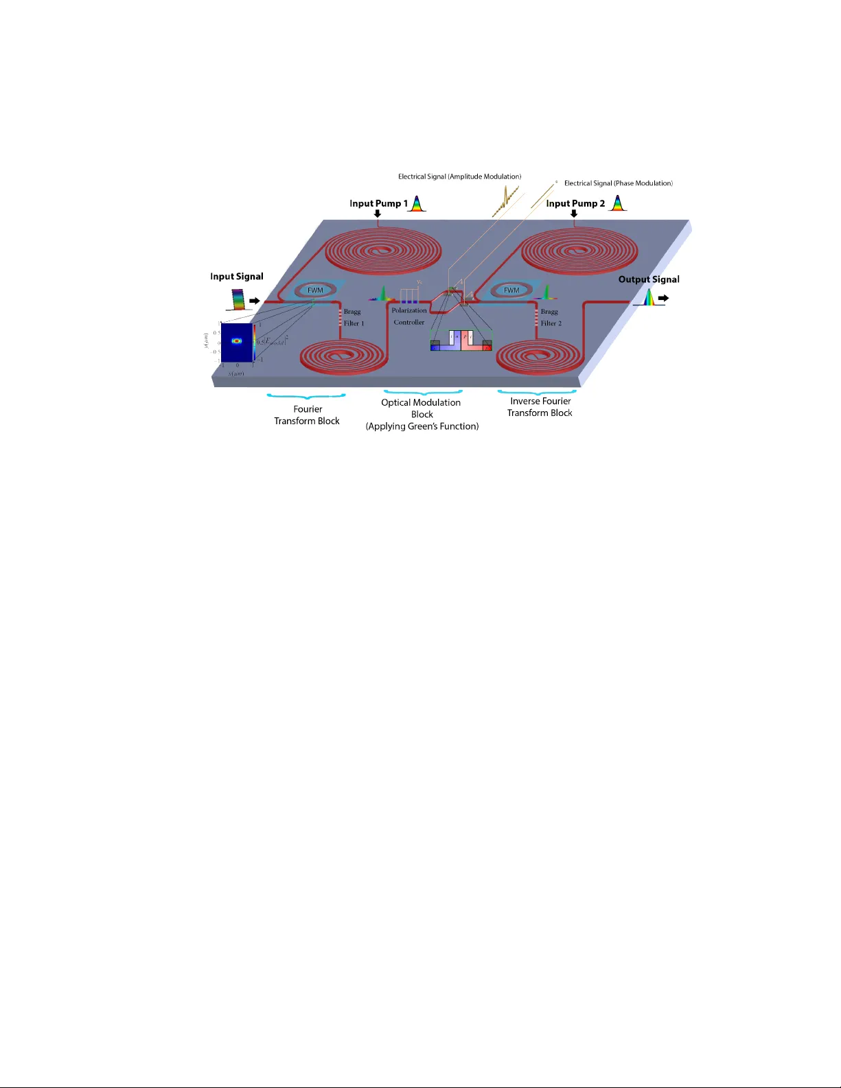
Loading comments...
Leave a Comment