📝 Original Info
- Title: Cost Modeling and Projection for Stacked Nanowire Fabric
- ArXiv ID: 1709.01965
- Date: 2017-11-13
- Authors: Researchers from original ArXiv paper
📝 Abstract
To continue scaling beyond 2-D CMOS with 3-D integration, any new 3-D IC technology has to be comparable or better than 2-D CMOS in terms of scalability, enhanced functionality, density, power, performance, cost, and reliability. Transistor-level 3-D integration carries the most potential in this regard. Recently, we proposed a stacked horizontal nanowire based transistor-level 3-D integration approach, called SN3D [1][2] that solves scaling challenges and achieves tremendous benefits with respect to 2-D CMOS while keeping manageable thermal profile. In this paper, we present the cost analysis of SN3D and show comparison with 2-D CMOS (2D), conventional TSV based 3-D (T3D) and Monolithic 3-D integrations (M3D). In our cost model, we capture the implications of manufacturing, circuit density, interconnects, bonding and heat in determining die cost, and evaluate how cost scales as transistor count increases. Since SN3D is a new 3-D IC fabric, based on our proposed manufacturing pathway[1] we assumed complexity of fabrication steps as proportionality constants in our cost estimation model. Our analysis revealed 86%, 72% and 74% reduction in area; 55%, 43% and 43% reduction in interconnects distribution and total interconnect length for SN3D, which largely contributed to 70%, 67% and 68% reduction in cost in comparison to 2D, T3D and M3D respectively.
💡 Deep Analysis
Deep Dive into Cost Modeling and Projection for Stacked Nanowire Fabric.
To continue scaling beyond 2-D CMOS with 3-D integration, any new 3-D IC technology has to be comparable or better than 2-D CMOS in terms of scalability, enhanced functionality, density, power, performance, cost, and reliability. Transistor-level 3-D integration carries the most potential in this regard. Recently, we proposed a stacked horizontal nanowire based transistor-level 3-D integration approach, called SN3D [1][2] that solves scaling challenges and achieves tremendous benefits with respect to 2-D CMOS while keeping manageable thermal profile. In this paper, we present the cost analysis of SN3D and show comparison with 2-D CMOS (2D), conventional TSV based 3-D (T3D) and Monolithic 3-D integrations (M3D). In our cost model, we capture the implications of manufacturing, circuit density, interconnects, bonding and heat in determining die cost, and evaluate how cost scales as transistor count increases. Since SN3D is a new 3-D IC fabric, based on our proposed manufacturing pathway[1
📄 Full Content
Naveen Kumar Macha, Mostafizur Rahman
Department of Computer Science & Electrical Engineering, University of Missouri Kansas City, MO, USA
E-mail: nmhw9@mail.umkc.edu, rahmanmo@umkc.edu
Abstract— To continue scaling beyond 2-D CMOS with 3-D
integration, any new 3-D IC technology has to be comparable or
better than 2-D CMOS in terms of scalability, enhanced
functionality, density, power, performance, cost, and reliability.
Transistor-level 3-D integration carries the most potential in this
regard. Recently, we proposed a stacked horizontal nanowire
based transistor-level 3-D integration approach, called SN3D
[1][2] that solves scaling challenges and achieves tremendous
benefits with respect to 2-D CMOS while keeping manageable
thermal profile. In this paper, we present the cost analysis of SN3D
and show comparison with 2-D CMOS, conventional TSV based
3-D (T3-D) and Monolithic 3-D (M3-D) integrations. In our cost
model, we capture the implications of manufacturing, circuit
density, interconnects, bonding and heat in determining die cost
and evaluate how cost scales as transistor count increases. Since,
SN3D is a new 3-D IC fabric, based on our proposed
manufacturing pathway [2] we assumed complexity of fabrication
steps as proportionality constants in our cost estimation model.
Our analysis revealed SN3D have 86% and 74% reduction in area;
55% and 43% reduction in interconnect distribution and total
interconnect length required; reduced metal layer requirement;
and 70% and 68% reduction in total cost in comparison to 2-D
CMOS and Monolithic 3-D (M3-D) integrations respectively.
Index Terms—3-D IC, 3-D CMOS, Fine-Grained 3-D, SN3D, 3-
D Manufacturing, 3-D cost, SN3D Cost
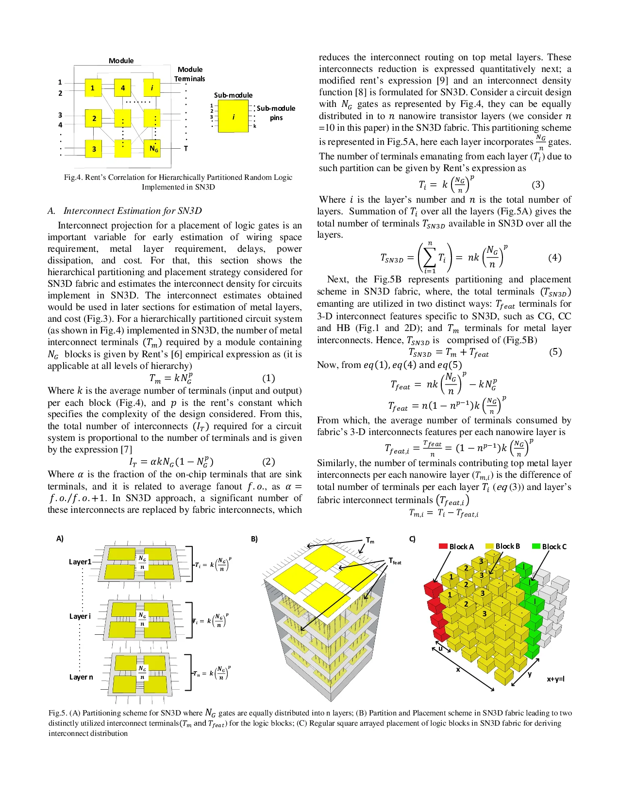
I. INTRODUCTION
Transistor-level 3-D integration is considered the most
promising direction for replacing 2-D CMOS due to its density
and performance benefits. Our proposal for transistor-level 3-
D integration called stacked horizontal nanowire based 3-D IC
fabric (SN3D), is based on stacked horizontal nanowires and
uses
architected
features
for
circuit
functionality,
interconnection, and thermal management. Previously we
reported huge gains with SN3D design [1-3]. In this paper, we
focus on cost aspects and show a detailed comparison with 2-D
CMOS, TSV based 3-D CMOS (T3-D) and monolithic 3-D
(M3-D) integrations.
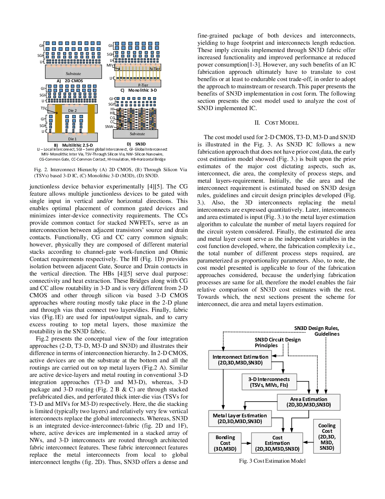
Fig. 1 shows core components of the fabric and overview of
circuit mapped SN3D fabric. Stacked suspended horizontal
nanowires (Fig. 1A) are the building blocks, which are
prefabricated, and predopped. Architected fabric components:
Gate-All-Around junctionless nanowire FETs (Fig. 1B),
Common Contact (CC- Fig. 1C.i), Common Gate (CG- Fig.
1C.ii), Horizontal Bridges (HB- Fig. 1C.iii), Horizontal
Insulation (HI-Fig. 1D) and Fabric Vias (FV- Fig. 1E) are
formed onto these nanowires through material deposition
techniques[4][5]. Active devices here are junctionless nanowire
transistors that do not require any doping variation for
Drain/Source/Channel regions. Previously we demonstrated
Cost Modeling and Projection for Stacked
Nanowire Fabric
A) Stacked Nanowires
C) Fabric Interconnect Features
(i) Common Contact
Contact
(Ni)
Gate
(TiN)
Gate
(Ti)
(ii) Common Gate
(iii) Horizontal Bridge
F) SN3D Fabric-View
Nanowire (Si)
B) Nanowire Transistor
NW Channel
Gate Oxide(HfO2)
Contact
Gate
(Ti/TiN)
Spacer
(Si3N4)
Contact
(Al)
Bridge
E) Vias
Nano-Vias
(W)
Horizontal
Isolation
(SU8/SiO2)
D) Horizontal Insulation (HI)
Substrate
Metal
Stack
Via
Insulation
Nanowire
Gate
Bridge
Common
Contact
Fig. 1: (A) Stacked Nanowires; (B) Junction-less Gate All Around Nanowire Transistor; (C) Fabric-Interconnects, (i) Common Contact (CC), (ii) Common Gate
(CG), (iii) Horizontal Bridge (HB); (D) Horizontal Insulation (HI); (E) Fabric-Vias; (F) SN3D Fabric-Overview
junctionless device behavior experimentally [4][5]. The CG
feature allows multiple junctionless devices to be gated with
single input in vertical and/or horizontal directions. This
enables optimal placement of common gated devices and
minimizes inter-device connectivity requirements. The CCs
provide common contact for stacked NWFETs, serve as an
interconnection between adjacent transistors’ source and drain
contacts. Functionally, CG and CC carry common signals;
however, physically they are composed of different material
stacks according to channel-gate work-function and Ohmic
Contact requirements respectively. The HI (Fig. 1D) provides
isolation between adjacent Gate, Source and Drain contacts in
the vertical direction. The HBs [4][5] serve dual purpose:
connectivity and heat extraction. These Bridges along with CG
and CC allow routability in 3-D and is very different from 2-D
CMOS and other through silicon via based 3-D CMOS
approaches where routing mostly take place in the 2-D plane
and through vias that connect two layers/dies. Finally, fabric
vias (Fig.1E) are used for input/output signals, and to
…(Full text truncated)…
📸 Image Gallery
Reference
This content is AI-processed based on ArXiv data.