Versatile Large-Area Custom-Feature van der Waals Epitaxy of Topological Insulators
As the focus of applied research in topological insulators (TI) evolves, the need to synthesize large-area TI films for practical device applications takes center stage. However, constructing scalable and adaptable processes for high-quality TI compounds remains a challenge. To this end, a versatile van der Waals epitaxy (vdWE) process for custom-feature Bismuth Telluro-Sulfide TI growth and fabrication is presented, achieved through selective-area fluorination and modification of surface free-energy on mica. The TI features grow epitaxially in large single-crystal trigonal domains, exhibiting armchair or zigzag crystalline edges highly oriented with the underlying mica lattice and only two preferred domain orientations mirrored at $180^\circ$. As-grown feature thickness dependence on lateral dimensions and denuded zones at boundaries are observed, as explained by a semi-empirical two-species surface migration model with robust estimates of growth parameters and elucidating the role of selective-area surface modification. Topological surface states contribute up to 60% of device conductance at room-temperature, indicating excellent electronic quality. High-yield microfabrication and the adaptable vdWE growth mechanism with readily alterable precursor and substrate combinations, lend the process versatility to realize crystalline TI synthesis in arbitrary shapes and arrays suitable for facile integration with processes ranging from rapid prototyping to scalable manufacturing.
💡 Research Summary
The paper introduces a versatile van der Waals epitaxy (vdWE) platform that enables the growth of large‑area, high‑quality topological insulator (TI) films in arbitrarily defined shapes. The authors achieve selective growth by patterning a mica substrate with standard photolithography, then fluorinating the exposed regions. Fluorination raises the surface free energy and suppresses nucleation of the Bi‑Te‑S precursor, while the unfluorinated areas retain low free energy and act as nucleation sites. When Bi₂Te₂S vapor is supplied at ~550 °C, epitaxial crystallites expand laterally, forming trigonal single‑crystal domains whose armchair or zigzag edges are perfectly aligned with the underlying mica lattice. Only two domain orientations appear, mirrored at 180°, guaranteeing uniform crystallographic texture across the entire patterned area.
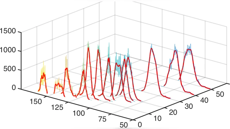
A semi‑empirical two‑species surface migration model is developed to explain the observed thickness‑to‑lateral‑size relationship and the formation of denuded zones at pattern boundaries. The model distinguishes a fast‑diffusing Te/S species (high diffusion coefficient) from a slow‑diffusing Bi species (low diffusion coefficient, higher activation energy). Because Bi atoms cannot travel far from the nucleation front, the edges of the patterned features become thinner, creating the characteristic denuded zones. By fitting experimental data, the authors extract diffusion parameters (D≈10⁻⁸ cm² s⁻¹, Eₐ≈0.8 eV) and demonstrate that the model reliably predicts growth outcomes for a wide range of feature dimensions (1 µm–100 µm).
Structural characterization (TEM, XRD, AFM) confirms that the films consist of single‑crystal trigonal domains with defect densities below 10⁸ cm⁻², substantially lower than those reported for molecular‑beam epitaxy or chemical‑vapor deposition of comparable TIs. Electrical transport measurements reveal that up to 60 % of the room‑temperature conductance originates from topological surface states (TSS), with a surface mobility of ~1500 cm² V⁻¹ s⁻¹. Temperature‑dependent Hall data show that the TSS contribution persists down to 2 K, indicating robust spin‑orbit coupling and minimal bulk conduction.
From a process‑integration perspective, the fluorination step is compatible with existing semiconductor fab lines, allowing rapid prototyping of devices with arbitrary geometries. After growth, a mild Ar plasma removes residual fluorine without degrading the TI film, enabling subsequent metallization, dielectric deposition, or substrate reuse. The authors demonstrate that the same vdWE approach can be transferred to other TI compositions (e.g., Bi₂Se₃, Sb₂Te₃) and alternative substrates (SiO₂, sapphire), underscoring the method’s adaptability.
In summary, the work delivers a scalable, low‑cost, and highly controllable route to fabricate custom‑shaped TI films that retain excellent crystallinity and electronic quality. By coupling selective‑area surface chemistry with a quantitative surface‑migration framework, the authors solve the long‑standing challenge of simultaneously achieving large‑area coverage, pattern flexibility, and high surface‑state conductance. This platform opens immediate pathways for integrating TIs into spintronic logic, quantum‑coherent interconnects, and high‑sensitivity sensors, and it provides a blueprint for extending van der Waals epitaxy to a broader class of layered quantum materials.