Investigation of Dependence between Time-zero and Time-dependent Variability in High-k NMOS Transistors
Bias Temperature Instability (BTI) is a major reliability concern in CMOS technology, especially with High dielectric constant (High-\k{appa}/HK) metal gate (MG) transistors. In addition, the time independent process induced variation has also increased because of the aggressive scaling down of devices. As a result, the faster devices at the lower threshold voltage distribution tail experience higher stress, leading to additional skewness in the BTI degradation. Since time dependent dielectric breakdown (TDDB) and stress-induced leakage current (SILC) in NMOS devices are correlated to BTI, it is necessary to investigate the effect of time zero variability on all these effects simultaneously. To that effect, we propose a simulation framework to model and analyze the impact of time-zero variability (in particular, random dopant fluctuations) on different aging effects. For small area devices (~1000 nm2) in 30nm technology, we observe significant effect of Random Dopant Fluctuation (RDF) on BTI induced variability ({\sigma}{\Delta}Vth). In addition, the circuit analysis reveals similar trend on the performance degradation. However, both TDDB and SILC show weak dependence on RDF. We conclude that the effect of RDF on Vth degradation cannot be disregarded in scaled technology and needs to be considered for variation tolerant circuit design.
💡 Research Summary
This paper investigates the interplay between time‑zero variability—specifically Random Dopant Fluctuation (RDF)—and time‑dependent aging mechanisms in high‑κ metal‑gate NMOS transistors fabricated in a 30 nm technology node. As device dimensions shrink, the statistical spread of dopant atoms becomes a dominant source of initial threshold‑voltage (Vth) variation. The authors argue that this initial spread directly influences the stress experienced by “fast” devices located on the low‑Vth tail of the distribution, thereby amplifying Bias Temperature Instability (BTI) degradation and potentially skewing overall reliability metrics.
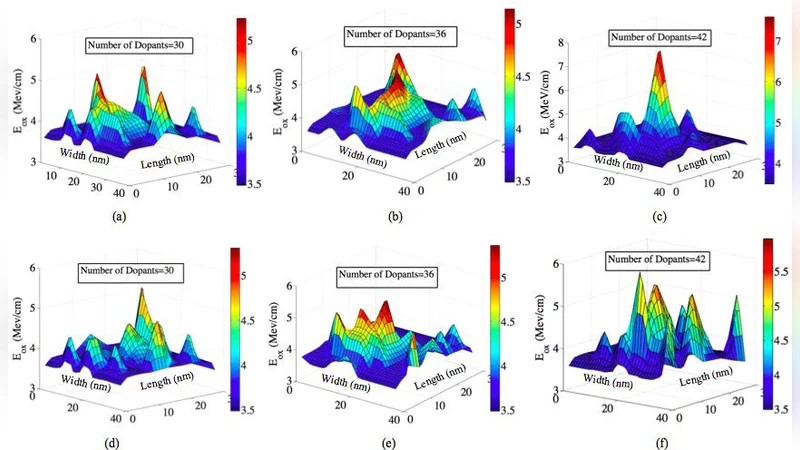
To quantify these effects, the authors develop a Monte‑Carlo‑based TCAD simulation framework. They generate a large ensemble of transistor instances, each with a random spatial distribution of dopant atoms that reproduces the measured σVth for a 1000 nm² device area. All devices are subjected to identical voltage‑temperature stress conditions, and the evolution of ΔVth due to BTI is tracked over time. In parallel, the same stress conditions are applied to evaluate Time‑Dependent Dielectric Breakdown (TDDB) and Stress‑Induced Leakage Current (SILC) for each instance, allowing a direct comparison of how RDF influences each aging phenomenon.
The simulation results reveal three key findings. First, RDF dramatically widens the initial Vth distribution; when σVth exceeds roughly 10 mV, the standard deviation of BTI‑induced ΔVth (σΔVth) rises by more than 30 %. This is attributed to the fact that low‑Vth devices experience higher electric fields under the same bias, accelerating trap generation and charge trapping processes that underlie BTI. Second, circuit‑level analysis shows that the amplified Vth spread translates into noticeable performance penalties: gate delay, dynamic power, and timing margins degrade, with worst‑case timing overheads reaching up to 15 % compared to a nominal design that ignores RDF. Third, both TDDB and SILC exhibit only a weak dependence on RDF. The statistical distribution of breakdown times (tBD) and leakage‑current growth rates remains essentially unchanged whether RDF is included or not, indicating that these mechanisms are governed primarily by the electric field and temperature rather than the initial dopant configuration.
From a design perspective, the authors argue that ignoring RDF in reliability budgeting can lead to under‑estimation of BTI‑related variability and, consequently, to insufficient timing margins in advanced nodes. They suggest that variation‑aware design techniques—such as adaptive body bias, voltage scaling, or statistical timing analysis—should be incorporated early in the design flow to mitigate the impact of RDF‑driven BTI spread. Conversely, because TDDB and SILC are less sensitive to RDF, traditional worst‑case field‑based reliability checks remain adequate for those failure modes.
In summary, the study demonstrates that in aggressively scaled high‑κ/metal‑gate technologies, time‑zero variability, especially RDF, is a critical contributor to BTI variability and overall circuit performance degradation, while its influence on TDDB and SILC is marginal. The findings underscore the necessity of integrating stochastic dopant‑fluctuation models into both device‑level simulations and system‑level design methodologies to achieve robust, variation‑tolerant circuits in future CMOS technologies.
Comments & Academic Discussion
Loading comments...
Leave a Comment