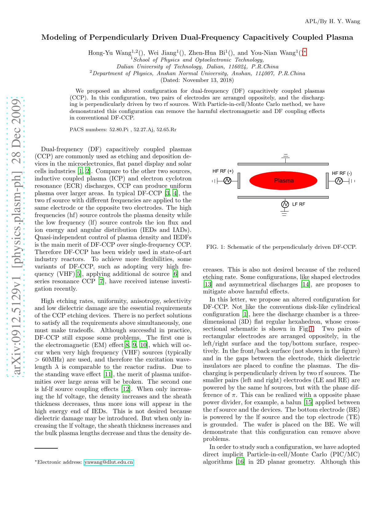
We proposed an altered configuration for dual-frequency (DF) capacitively coupled plasmas (CCP). In this configuration, two pairs of electrodes are arranged oppositely, and the discharging is perpendicularly driven by two rf sources. With Particle-in-cell/Monte Carlo method, we have demonstrated this configuration can remove the harmful electromagnetic and DF coupling effects in conventional DF-CCP.
Deep Dive into Modeling of Perpendicularly Driven Dual-Frequency Capacitively Coupled Plasma.
We proposed an altered configuration for dual-frequency (DF) capacitively coupled plasmas (CCP). In this configuration, two pairs of electrodes are arranged oppositely, and the discharging is perpendicularly driven by two rf sources. With Particle-in-cell/Monte Carlo method, we have demonstrated this configuration can remove the harmful electromagnetic and DF coupling effects in conventional DF-CCP.
Dual-frequency (DF) capacitively coupled plasmas (CCP) are commonly used as etching and deposition devices in the microelectronics, flat panel display and solar cells industries [1,2]. Compare to the other two sources, inductive coupled plasma (ICP) and electron cyclotron resonance (ECR) discharges, CCP can produce uniform plasma over larger areas. In typical DF-CCP [3,4], the two rf source with different frequencies are applied to the same electrode or the opposite two electrodes. The high frequencies (hf) source controls the plasma density while the low frequency (lf) source controls the ion flux and ion energy and angular distribution (IEDs and IADs). Quasi-independent control of plasma density and IEDFs is the main merit of DF-CCP over single-frequency CCP. Therefore DF-CCP has been widely used in state-of-art industry reactors. To achieve more flexibilities, some variants of DF-CCP, such as adopting very high frequency (VHF) [5], applying additional dc source [6] and series resonance CCP [7], have received intense investigation recently.
High etching rates, uniformity, anisotropy, selectivity and low dielectric damage are the essential requirements of the CCP etching devices. There is no perfect solutions to satisfy all the requirements above simultaneously, one must make tradeoffs. Although successful in practice, DF-CCP still expose some problems. The first one is the electromagnetic (EM) effect [8,9,10], which will occur when very high frequency (VHF) sources (typically > 60MHz) are used, and therefore the excitation wavelength λ is comparable to the reactor radius. Due to the standing wave effect [11], the merit of plasma uniformities over large areas will be broken. The second one is hf-lf source coupling effects [12]. When only increasing the hf voltage, the density increases and the sheath thickness decreases, thus more ions will appear in the high energy end of IEDs. This is not desired because dielectric damage may be introduced. But when only increasing the lf voltage, the sheath thickness increases and the bulk plasma lengths decrease and thus the density de- * Electronic address: ynwang@dlut.edu.cn creases. This is also not desired because of the reduced etching rate. Some configurations, like shaped electrodes [13] and asymmetrical discharges [14], are proposes to mitigate above harmful effects.
In this letter, we propose an altered configuration for DF-CCP. Not like the conventions disk-like cylindrical configuration [1], here the discharge chamber is a threedimensional (3D) flat regular hexahedron, whose crosssectional schematic is shown in Fig. 1. Two pairs of rectangular electrodes are arranged oppositely, in the left/right surface and the top/bottom surface, respectively. In the front/back surface (not shown in the figure) and in the gaps between the electrode, thick dielectric insulators are placed to confine the plasmas. The discharging is perpendicularly driven by two rf sources. The smaller pairs (left and right) electrodes (LE and RE) are powered by the same hf sources, but with the phase difference of π. This can be realized with a opposite phase power divider, for example, a balun [15] applied between the rf source and the devices. The bottom electrode (BE) is powered by the lf source and the top electrode (TE) is grounded. The wafer is placed on the BE. We will demonstrate that this configuration can remove above problems.
In order to study such a configuration, we have adopted direct implicit Particle-in-cell/Monte Carlo (PIC/MC) algorithms [16] in 2D planar geometry. Although this configuration is inherently 3D, due to the confinement by the insulators, the plasma is uniform between the side-wall insulators and thus 2D model is sufficient, if the front/back spacing is large. The details of the algorithms are described elsewhere [17], therefore we will only present the simulation parameters here. The BE and TE lengths are X = 8cm, and the LE and RE lengths are Y = 1.5cm, therefore we have the four gaps of 0.25cm. The hf sources of ω hf = 60MHz and V hf = 50V or 100V are applied to LE and RE, with the phase difference of π. The lf sources of ω lf = 2MHz and V lf = 50V or 100V are applied to BE. In the gaps, the instant potentials are linearly interpolated. Argon gas is used with the pressure of 10mTorr and temperature of 300K. We consider elastic, excitation and ionization collisions for electrons and elastic and charge transfer collisions for Ar + ions, respectively. Square cells are used, thus X direction is uniformly divided to 256 cells and Y direction divided to 64 cells. The space and time steps are fixed to all simulations, ∆x = 0.02/64m, ∆t e = ∆t i = 0.5 × 10 -10 s. All results are given by averaging over one lf period after reaching equilibrium of 1000 rf periods. Because the diodes areas are equal for X / Y separately and only the ideal voltage sources in the external circuit, we did not consider the external circuit and the self-biasing for simpleness.
The aver
…(Full text truncated)…
This content is AI-processed based on ArXiv data.