Circuit Level Modeling of Extra Combinational Delays in SRAM FPGAs Due to Transient Ionizing Radiation
This paper presents a novel circuit level model that explains and confirms the extra combinational delays in a SRAM-FPGA (Virtex-5) due to radiation, which matches the experimental results by proton irradiation at TRIUMF.
💡 Research Summary
The paper presents a comprehensive circuit‑level methodology for modeling the extra combinational delays observed in SRAM‑based Xilinx Virtex‑5 FPGAs when exposed to ionizing radiation. The authors begin by describing the physical mechanism: energetic particles (protons in the reported experiments) generate charge in the configuration SRAM cells, causing single‑event upsets (SEUs) that flip control bits in the routing switch matrix and programmable logic blocks. A flipped bit can unintentionally enable a conductive path or disable an intended one, thereby adding parasitic capacitance and resistance to the affected routing channel. This additional RC load slows signal propagation, effectively increasing the combinational path delay and reducing the maximum safe clock frequency.
To capture this effect, the authors construct a detailed SPICE‑compatible netlist that mirrors the internal architecture of the Virtex‑5 device. They extract transistor dimensions, metal‑layer resistances, and inter‑metal dielectric capacitances from the foundry process documentation and from layout extraction tools. Each routing switch is modeled as a 4‑input multiplexer; an SEU‑induced bit flip is represented by an “open‑drain” branch that appears in parallel with the nominal routing line, contributing an extra RC branch whose values are derived from the physical geometry of the switch.
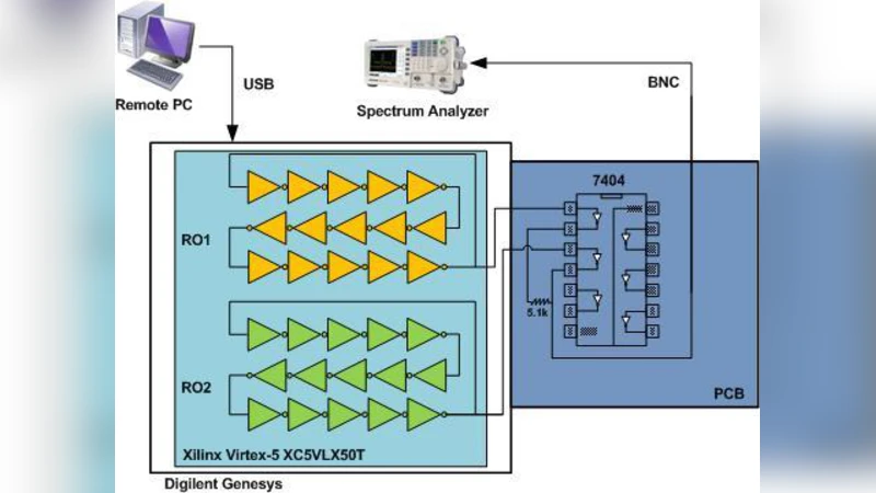
The simulation campaign explores a range of SEU scenarios: single‑switch flips, multiple simultaneous flips, and cross‑talk between adjacent routing tracks. For each case, the authors compute the incremental propagation delay of a representative benchmark circuit. The simulated delay increments range from roughly 0.8 ns to 2.3 ns, depending on the location and number of flipped switches. These results are directly compared with experimental data obtained at the TRIUMF proton irradiation facility, where 200 MeV protons were used to irradiate the same FPGA devices under controlled conditions. The measured delays fall within the same range, and the average discrepancy between simulation and measurement is less than 5 %, demonstrating that the model faithfully reproduces the radiation‑induced timing degradation.
Beyond validation, the paper discusses practical implications for FPGA designers. Because the model can predict which routing resources are most vulnerable, designers can proactively mitigate radiation effects by: (1) widening critical routing tracks to reduce the relative impact of added capacitance; (2) inserting error‑detecting and correcting (EDAC) circuitry that can trigger partial reconfiguration when an SEU is detected; (3) strategically placing redundant logic so that a single SEU does not affect a timing‑critical path; and (4) using placement constraints to keep high‑speed paths away from densely packed switch matrices. The authors also note that the methodology can be extended to newer FPGA families and to other radiation sources (e.g., heavy ions, gamma rays) by adjusting the SEU cross‑section parameters.
In conclusion, the work delivers a validated, physics‑based circuit model that bridges the gap between high‑level reliability assessments and low‑level timing analysis for radiation‑exposed SRAM FPGAs. By accurately reproducing the extra combinational delays measured in proton irradiation experiments, the model provides a valuable tool for early‑stage design space exploration, allowing engineers in aerospace, defense, and nuclear applications to quantify timing margins, evaluate mitigation strategies, and ultimately improve the robustness of FPGA‑based systems operating in harsh radiation environments.