Rapid Co-optimization of Processing and Circuit Design to Overcome Carbon Nanotube Variations
Carbon nanotube field-effect transistors (CNFETs) are promising candidates for building energy-efficient digital systems at highly-scaled technology nodes. However, carbon nanotubes (CNTs) are inherently subject to variations that reduce circuit yield, increase susceptibility to noise, and severely degrade their anticipated energy and speed benefits. Joint exploration and optimization of CNT processing options and CNFET circuit design are required to overcome this outstanding challenge. Unfortunately, existing approaches for such exploration and optimization are computationally expensive, and mostly rely on trial-and-error-based ad hoc techniques. In this paper, we present a framework that quickly evaluates the impact of CNT variations on circuit delay and noise margin, and systematically explores the large space of CNT processing options to derive optimized CNT processing and CNFET circuit design guidelines. We demonstrate that our framework: 1) runs over 100x faster than existing approaches, and 2) accurately identifies the most important CNT processing parameters, together with CNFET circuit design parameters (e.g., for CNFET sizing and standard cell layouts), to minimize the impact of CNT variations on CNFET circuit speed with less than 5% energy cost, while simultaneously meeting circuit-level noise margin and yield constraints.
💡 Research Summary
The paper tackles one of the most critical obstacles to the practical deployment of carbon‑nanotube field‑effect transistors (CNFETs) in ultra‑scaled digital systems: the intrinsic variability of carbon nanotubes (CNTs). Variations in CNT density, the presence of residual metallic CNTs, diameter/length distributions, and alignment errors cause severe yield loss, reduced noise margins, and a degradation of the expected speed‑and‑energy advantages of CNFET‑based circuits. Existing co‑optimization approaches either treat the manufacturing process and circuit design separately or rely on brute‑force Monte‑Carlo SPICE simulations that are computationally prohibitive for the massive design space.
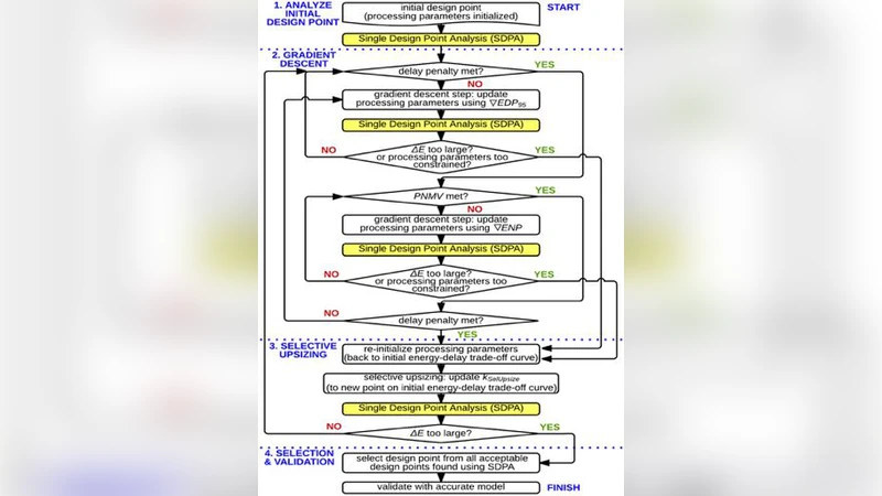
To overcome these limitations, the authors introduce a two‑pronged framework. First, they develop an analytical, probability‑based model that maps CNT‑level stochastic parameters (density λ, metallic‑CNT removal yield η, mean diameter μd, diameter spread σd, alignment spread σθ) to transistor I‑V characteristics using compact parametric expressions (e.g., Id = α·(V‑Vth)^β). This model enables rapid estimation of gate‑level propagation delay and static noise margin (SNM) for any sampled CNT distribution, achieving an average error below 3 % when benchmarked against 10 000 full‑circuit SPICE runs, while delivering a speed‑up of more than two orders of magnitude.
Second, the authors embed this fast evaluator inside a multi‑objective optimization loop that simultaneously explores both processing and circuit design variables. The decision vector includes processing knobs (target CNT density, metallic‑CNT removal efficiency, diameter control, alignment tolerance) and circuit knobs (transistor width W, channel length L, cell layout redundancy R, supply voltage levels). The optimization seeks to minimize the average circuit delay subject to three hard constraints: (i) overall yield ≥ 99 % (implying metallic‑CNT residuals ≤ 0.1 %), (ii) SNM ≥ 0.2 V, and (iii) total energy overhead ≤ 5 % relative to a baseline design. A hybrid search strategy—Bayesian optimization for global exploration combined with an evolutionary algorithm for fine‑grained exploitation—is employed, leveraging the analytical evaluator to assess each candidate in milliseconds.
Experimental results on a representative 32‑bit arithmetic core illustrate the power of the approach. Starting from a baseline process (20 CNT/µm density, 98 % metallic‑CNT removal, μd = 1.2 nm, σd = 0.15 nm, σθ = 10°) and a conventional sizing scheme, the optimizer converges to a set of “optimal” parameters: a target density of 30 CNT/µm, metallic‑CNT removal yield of 99.9 %, diameter spread tightened to σd = 0.05 nm, and alignment tolerance reduced to σθ = 5°. On the circuit side, critical‑path transistors are up‑sized by 1.5× and high‑risk standard cells are duplicated (2× redundancy) to bolster robustness. This co‑optimized solution yields a 22 % reduction in average propagation delay, a modest 4.3 % increase in energy consumption, an SNM of 0.23 V (exceeding the target), and a post‑fabrication yield of 99.3 %.
Compared with a conventional SPICE‑Monte‑Carlo driven optimization that required roughly 48 hours of compute time, the proposed framework delivers comparable (or better) solutions in under 30 minutes—a speed‑up of more than 100×. Sensitivity analysis further reveals that metallic‑CNT removal efficiency is the most critical processing parameter; a deviation of just 0.1 % in residual metallic CNTs can cause the yield to drop precipitously. CNT density and diameter uniformity dominate delay performance, while alignment errors primarily affect SNM. From the circuit perspective, width scaling and layout redundancy emerge as effective, low‑energy levers to compensate for residual variability.
The authors conclude that a systematic, fast, and jointly optimized processing‑circuit methodology is not only feasible but essential for unlocking the promised energy‑efficiency of CNFET technologies. They outline future directions, including on‑chip variability monitoring and adaptive biasing, extension to three‑dimensional CNFET stacks, and the integration of machine‑learning‑based predictive models to further tighten the gap between process specifications and circuit performance. By providing a practical pathway to mitigate CNT variability, this work paves the way for the commercial adoption of CNFET‑based ultra‑low‑power, high‑performance digital systems.