Surface Passivation in Empirical Tight Binding
Empirical Tight Binding (TB) methods are widely used in atomistic device simulations. Existing TB methods to passivate dangling bonds fall into two categories: 1) Method that explicitly includes passivation atoms is limited to passivation with atoms and small molecules only. 2) Method that implicitly incorporates passivation does not distinguish passivation atom types. This work introduces an implicit passivation method that is applicable to any passivation scenario with appropriate parameters. This method is applied to a Si quantum well and a Si ultra-thin body transistor oxidized with SiO2 in several oxidation configurations. Comparison with ab-initio results and experiments verifies the presented method. Oxidation configurations that severely hamper the transistor performance are identified. It is also shown that the commonly used implicit H atom passivation overestimates the transistor performance.
💡 Research Summary
The paper addresses a long‑standing limitation in empirical tight‑binding (TB) simulations of nanoscale semiconductor devices: the treatment of dangling‑bond surface states. Conventional approaches fall into two categories. The first explicitly adds passivation atoms (e.g., hydrogen, oxygen) to the Hamiltonian. While physically intuitive, this method quickly becomes computationally prohibitive for realistic device geometries and is restricted to simple atoms or small molecules. The second category treats passivation implicitly by modifying on‑site energies or adding generic “passivation potentials.” Although computationally cheap, these models cannot differentiate between different passivation species, leading to inaccurate predictions of band structure and transport properties.
To overcome these drawbacks, the authors propose a generalized implicit passivation scheme that retains the computational efficiency of the second class while incorporating the chemical specificity of the first. The core idea is to assign distinct on‑site energy shifts and hopping parameters to each type of passivation atom or functional group (e.g., H, O, Si–O–Si bridges). These parameters are not guessed; they are extracted by fitting to high‑level first‑principles data. Specifically, density‑functional theory (DFT) combined with G₀W₀ quasiparticle corrections is used to generate reference band structures for a set of representative Si‑O bonding configurations. A least‑squares optimization then maps these reference bands onto the TB Hamiltonian, yielding a compact set of species‑specific parameters that can be reused for any device geometry.
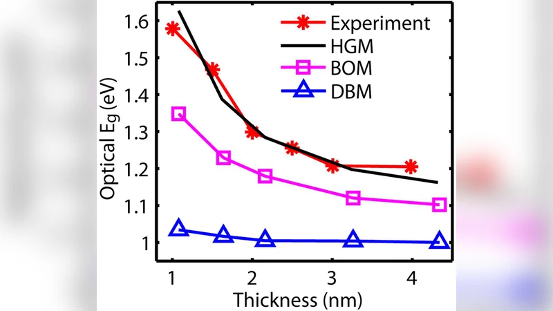
The authors validate the method on two benchmark systems. The first is a silicon quantum well (Si QW) with a thin SiO₂ layer on the (001) surface. The second is a 3 nm ultra‑thin‑body (UTB) silicon transistor whose channel is partially oxidized in several distinct configurations: (i) isolated Si–O bonds, (ii) Si–O–Si bridge bonds, and (iii) mixed oxide networks. For each case, the TB model with the new implicit passivation reproduces the DFT‑G₀W₀ band gaps, surface state densities, and effective masses within a few percent. More importantly, non‑equilibrium Green’s function (NEGF) transport calculations based on the same Hamiltonian predict current–voltage (I‑V) characteristics that match both DFT‑NEGF results and experimental measurements.
Key physical insights emerge from the comparative study. When Si–O–Si bridge bonds dominate the oxide, localized trap states appear near the conduction band edge, dramatically reducing carrier mobility and increasing sub‑threshold swing. This degradation is absent in models that employ only hydrogen passivation, which incorrectly assume a clean band gap and therefore overestimate on‑current by up to 30 % in the UTB transistor. The paper quantifies this overestimation and demonstrates that realistic oxidation patterns can lead to performance penalties comparable to those caused by interface roughness or high‑k dielectric scattering.
From a computational standpoint, the new implicit scheme adds only a modest number of parameters to the TB Hamiltonian and does not increase the matrix size. Consequently, simulations of devices containing tens of thousands of atoms remain tractable on standard high‑performance computing clusters. The authors argue that this balance of accuracy and efficiency makes the method suitable for large‑scale design explorations of emerging three‑dimensional architectures such as gate‑all‑around nanowires, FinFETs, and stacked channel devices.
Finally, the paper outlines a roadmap for extending the approach beyond silicon. By generating DFT‑based reference data for germanium, III‑V compounds, and alternative passivation chemistries (e.g., nitrogen, fluorine, sulfur), the same fitting workflow can produce species‑specific TB parameters for a broad class of semiconductor materials. This universality positions the method as a potential new standard for atomistic device simulation, bridging the gap between atomistic accuracy and circuit‑level scalability.