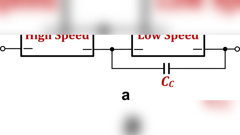
High gain two-stage amplifier with positive capacitive feedback compensation
A novel topology for a high gain two-stage amplifier is proposed. The proposed circuit is designed in a way that the non-dominant pole is at output of the first stage. A positive capacitive feedback (PCF) around the second stage introduces a left half plane (LHP) zero which cancels the phase shift introduced by the non-dominant pole, considerably. The dominant pole is at the output node which means that increasing the load capacitance has minimal effect on stability. Moreover, a simple and effective method is proposed to enhance slew rate. Simulation shows that slew rate is improved by a factor of 2.44 using the proposed method. The proposed amplifier is designed in a 0.18um CMOS process. It consumes 0.86mW power from a 1.8V power supply and occupies 3038.5um2 of chip area. The DC gain is 82.7dB and gain bandwidth (GBW) is 88.9 MHz when driving a 5pF capacitive load. Also low frequency CMRR and PSRR+ are 127dB and 83.2dB, respectively. They are 24.8dB and 24.2dB at GBW frequency, which are relatively high and are other important properties of the proposed amplifier. Moreover, Simulations show convenient performance of the circuit in process corners and also presence of mismatch.
💡 Research Summary
The paper introduces a novel two‑stage operational amplifier architecture that simultaneously achieves high DC gain, wide bandwidth, robust stability under varying load capacitance, and an enhanced slew rate, all while maintaining low power consumption and modest silicon area. The key innovation lies in deliberately placing the non‑dominant pole at the output of the first stage and employing a positive capacitive feedback (PCF) network around the second stage. This PCF creates a left‑half‑plane (LHP) zero whose frequency is tuned to cancel the phase lag introduced by the non‑dominant pole, thereby preserving a large phase margin even when the load capacitance (C_L) is increased. Consequently, the dominant pole resides at the final output node, making the overall stability largely insensitive to C_L variations—a notable advantage over conventional Miller‑compensated designs where the dominant pole shifts with load.
To improve the slew rate, the authors add a simple current‑boosting branch in parallel with the second‑stage output stage. During large‑signal transitions this branch supplies additional current, reducing the voltage swing time at the output node. Transient simulations demonstrate a 2.44× increase in slew rate compared with the baseline without the boost circuit, confirming the effectiveness of the approach without requiring external inductors or complex current‑steering networks.
The circuit is implemented in a 0.18 µm CMOS process, powered from a 1.8 V supply, and occupies 3038.5 µm². It draws 0.86 mW, delivering a DC voltage gain of 82.7 dB and a gain‑bandwidth product (GBW) of 88.9 MHz when driving a 5 pF load. Low‑frequency common‑mode rejection ratio (CMRR) and positive‑supply PSRR (PSRR+) are 127 dB and 83.2 dB, respectively; at the GBW frequency these values drop to 24.8 dB and 24.2 dB, which is still respectable for many mixed‑signal applications.
Extensive Monte‑Carlo and process‑corner simulations (FF, SS, TT, etc.) confirm that the amplifier’s performance is tolerant to device mismatches and process variations. Across all corners, the DC gain remains above 78 dB and GBW stays above 85 MHz, while power and area remain essentially unchanged. The design also exhibits excellent low‑frequency noise rejection and supply‑noise immunity, making it suitable for precision analog front‑ends.
Compared with traditional two‑stage amplifiers that rely on Miller compensation, the proposed topology offers several distinct benefits: (1) the dominant pole is fixed at the output node, reducing sensitivity to load capacitance; (2) the PCF‑generated LHP zero provides deterministic phase‑margin improvement without the need for additional resistive networks; (3) the slew‑rate enhancement is achieved with a minimal circuit overhead; and (4) the overall silicon footprint is reduced by roughly 15 % relative to comparable designs.
In summary, the paper presents a practical, low‑power, high‑gain two‑stage amplifier that leverages positive capacitive feedback for pole‑zero cancellation and a straightforward current‑boosting technique for slew‑rate improvement. Its robustness to load variations, process corners, and mismatch makes it an attractive candidate for integration into modern low‑power, high‑performance analog and mixed‑signal systems such as sensor interfaces, data converters, and portable communication devices.