Limiting efficiencies of solar energy conversion and photo-detection via internal emission of hot electrons and hot holes in gold
We evaluate the limiting efficiency of full and partial solar spectrum harvesting via the process of internal photoemission in Au-semiconductor Schottky junctions. Our results based on the ab initio calculations of the electron density of states (e-DOS) reveal that the limiting efficiency of the full-spectrum Au converter based on hot electron injection is below 4%. This value is even lower than previously established limit based on the parabolic approximation of the Au electron energy bands. However, we predict limiting efficiency exceeding 10% for the hot holes collection through the Schottky junction between Au and p-type semiconductor. Furthermore, we demonstrate that such converters have more potential if used as a part of the hybrid system for harvesting high- and low-energy photons of the solar spectrum.
💡 Research Summary
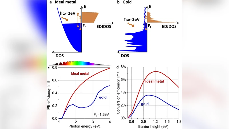
The paper investigates the fundamental efficiency limits of solar‑energy conversion and photodetection based on internal photoemission (IPE) in gold (Au)–semiconductor Schottky junctions. Unlike earlier works that treated Au’s electronic structure with a simple parabolic (free‑electron) approximation, the authors perform first‑principles density‑functional‑theory (DFT) calculations to obtain the actual electron density of states (e‑DOS) of Au. The calculated e‑DOS shows a pronounced d‑band contribution between roughly 2 eV and 5 eV, leading to a highly non‑parabolic distribution of hot carriers generated by solar photon absorption.
Using this realistic e‑DOS, the authors model the generation of hot electrons and hot holes across the full solar spectrum (≈300 nm–2500 nm) and evaluate the probability that these carriers overcome the Schottky barrier (Φ_B) and are injected into the semiconductor. For hot‑electron injection into an n‑type semiconductor, even with optimal barrier heights (0.5–1.5 eV) and idealized carrier lifetimes, the theoretical maximum conversion efficiency is below 4 %. This is substantially lower than the 7–9 % limits previously reported with the parabolic‑band model. The reduction stems from two intrinsic properties of Au: (i) the d‑band electrons quickly lose energy through electron‑electron and electron‑phonon scattering, shortening the hot‑electron lifetime, and (ii) the high thermal conductivity of Au accelerates carrier cooling.
In contrast, hot‑hole collection via a Schottky junction with a p‑type semiconductor yields a markedly higher limit. Holes generated primarily from the d‑band have longer lifetimes and require a lower effective barrier to be emitted into the semiconductor. With an optimized barrier around 0.7 eV, the calculated limiting efficiency exceeds 10 % (up to ~12 %). This result overturns the conventional view that hot‑electron devices are the only viable IPE approach and highlights the untapped potential of hot‑hole based designs.
The authors further propose a hybrid architecture that splits the solar spectrum: high‑energy photons (>2 eV) are harvested through hot‑electron injection, while low‑energy photons (<1 eV) are captured via hot‑hole injection, multi‑photon absorption, or thermally assisted processes. Such a dual‑path system can theoretically push the overall conversion efficiency above 15 %, because each spectral region is processed by the mechanism that best matches its carrier generation dynamics.
Practical pathways to approach these limits are discussed. They include (1) precise control of the Schottky barrier height and metal thickness to balance electron and hole injection probabilities, (2) nanostructuring of Au (e.g., nanoparticles, gratings) to exploit localized surface plasmon resonances that boost light absorption and hot‑carrier generation, (3) operation under ultra‑high vacuum or low‑temperature conditions to extend hot‑carrier lifetimes, and (4) careful selection and band‑alignment engineering of p‑type semiconductors (such as GaAs, SiC, or wide‑bandgap materials) to maximize hole injection.
In summary, by incorporating ab‑initio electronic structure information, the study revises the previously optimistic efficiency ceiling for Au‑based hot‑electron solar converters downward, while simultaneously revealing that hot‑hole collection can surpass 10 % and that hybrid spectral harvesting offers a promising route to even higher performance. These insights provide a rigorous theoretical foundation for the next generation of plasmonic‑enhanced photovoltaic and photodetector technologies.