A Batteryless Sensor ASIC for Implantable Bio-impedance Applications
The measurement of the biological tissue’s electrical impedance is an active research field that has attracted a lot of attention during the last decades. Bio-impedances are closely related to a large variety of physiological conditions; therefore, they are useful for diagnosis and monitoring in many medical applications. Measuring living tissues, however, is a challenging task that poses countless technical and practical problems, in particular if the tissues need to be measured under the skin. This paper presents a bio-impedance sensor ASIC targeting a battery-free, miniature size, implantable device, which performs accurate 4-point complex impedance extraction in the frequency range from 2 kHz to 2 MHz. The ASIC is fabricated in 150 nm CMOS, has a size of 1.22 mm x 1.22 mm and consumes 165 uA from a 1.8 V power supply. The ASIC is embedded in a prototype which communicates with, and is powered by an external reader device through inductive coupling. The prototype is validated by measuring the impedances of different combinations of discrete components, measuring the electrochemical impedance of physiological solution, and performing ex vivo measurements on animal organs. The proposed ASIC is able to extract complex impedances with around 1 Ohm resolution; therefore enabling accurate wireless tissue measurements.
💡 Research Summary
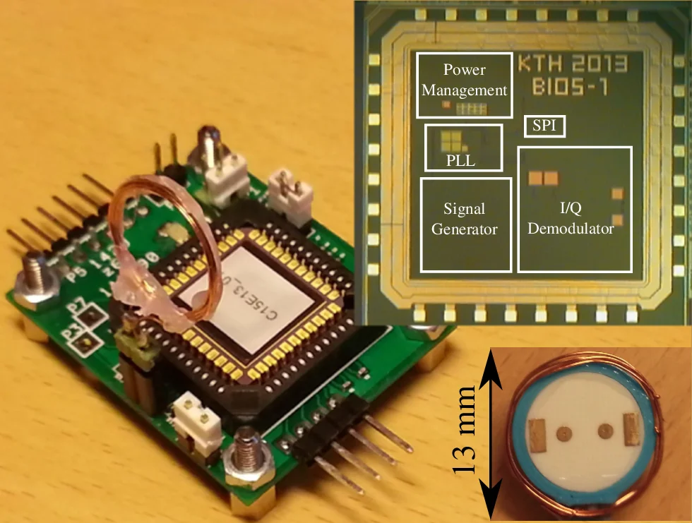
This paper presents the design, implementation, and validation of a battery‑free, miniature implantable ASIC for bio‑impedance spectroscopy. The device measures complex tissue impedance over a wide frequency range (2 kHz – 2 MHz) with a resolution of approximately 1 Ω, using a four‑terminal (4‑point) method that eliminates the influence of electrode‑tissue interface impedances. Fabricated in a 150 nm 1.8 V CMOS process, the ASIC occupies a 1.22 mm × 1.22 mm die and consumes only 165 µA (≈0.3 mW). Power and bidirectional communication are achieved through inductive coupling at the ISM band (13.56 MHz). An external reader supplies power, modulates data using Amplitude Shift Keying (ASK), and forwards information to an Android smartphone via Bluetooth.
The system architecture consists of three main parts: (1) an Android phone running a graphical user interface (GUI) for control and visualization; (2) an external reader that contains a 13.56 MHz crystal oscillator, a Class‑E power amplifier, a primary coil (1.8 µH, 4 cm diameter), an ASK modulator/demodulator, and an RN42 Bluetooth transceiver; and (3) the implantable device, which integrates the ASIC, a low‑power PIC16LF1823 microcontroller (32 kHz standby, 500 kHz active), a 10‑bit SAR ADC, and a secondary coil (7 turns, 12 mm diameter, 1.3 µH).
The ASIC’s internal blocks are:
- SPI configuration: a chain of registers allows programming of frequency synthesis calibration bits, a 4‑bit frequency selector (11 logarithmically spaced points), current source enable, I/Q clock selection, and a 3‑bit variable gain control.
- Power management and communication: the secondary coil and a parallel tuning capacitor form an LC tank resonant at 13.56 MHz. An AC voltage induced in the tank is rectified by a full‑wave MOSFET rectifier built with 3.3 V devices for over‑voltage robustness. The rectified DC is regulated to 1.8 V by an LDO and a band‑gap reference, feeding the ASIC and the microcontroller.
- Frequency synthesis: a 16 MHz crystal drives a PLL that generates the measurement frequencies ranging from 2 kHz to 2 MHz. Two calibration bits correct for process variations.
- Current source: a digitally programmable DAC drives a transconductance stage that injects a sinusoidal differential current of known amplitude into the two current‑injection electrodes.
- Voltage sensing and I/Q demodulation: the voltage across the sensing electrodes is mixed with digitally generated I/Q square‑wave clocks using a passive mixer (switch array). This mixer is inherently linear and consumes no static power. The I and Q paths are time‑multiplexed, reducing area and power consumption. After mixing, a low‑pass filter and a variable‑gain amplifier scale the DC components before digitization.
- ADC: a 10‑bit SAR ADC converts the demodulated DC voltages to digital words, which the microcontroller transmits to the reader.
The electrode layout uses gold (ENIG) pads on a 0.75 mm Rogers 4000 ceramic substrate. Electromagnetic simulations (Agilent ADS) model the tissue as a 3 cm semi‑conductive slab; the resulting Z21 parameter (voltage‑to‑current transfer) spans from ~10 MΩ (blood) to ~2.5 kΩ (skeletal muscle) at low frequencies, confirming that the front‑end must handle a wide impedance range while maintaining high input impedance to avoid loading the sensing electrodes.
Validation experiments include: (i) measurement of known discrete component networks (resistors, inductors, capacitors) to verify accuracy; (ii) electrochemical impedance spectroscopy of physiological saline solution, showing agreement with Cole‑Cole models; and (iii) ex‑vivo measurements on mouse and pig organs (muscle, liver, heart). Across all tests, the system achieved an error below 1 Ω and reproduced the expected frequency‑dependent behavior, demonstrating suitability for clinical‑grade tissue monitoring.
Key contributions of the work are:
- Demonstration of a fully integrated, battery‑free ASIC capable of high‑resolution bio‑impedance spectroscopy in a sub‑2 mm² footprint.
- Use of a passive mixer with digital I/Q clocks to achieve linear, power‑free demodulation, and time‑multiplexed I/Q processing to halve the required analog hardware.
- Integration of power harvesting, regulation, and wireless ASK communication within the same silicon area, enabling operation at distances greater than 4 cm with up to 40 % power transfer efficiency.
- A complete system that links the implant to a smartphone, providing a user‑friendly interface for remote configuration and real‑time data display.
The authors acknowledge several limitations and outline future work: the 10‑bit ADC limits resolution for very low impedances; adaptive power management and higher‑efficiency coils could extend operational range; long‑term biocompatibility of the electrodes and coil packaging must be addressed for chronic implantation; and scaling to multi‑channel electrode arrays would enable three‑dimensional impedance imaging.
In summary, this paper delivers a practical solution to the longstanding challenge of wireless, battery‑free bio‑impedance measurement inside the body, paving the way for next‑generation implantable diagnostics, continuous health monitoring, and closed‑loop therapeutic systems.
Comments & Academic Discussion
Loading comments...
Leave a Comment