Design and Simulation of Molecular Nonvolatile Single-Electron Resistive Switches
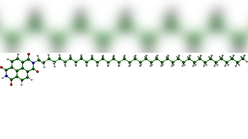
We have carried out a preliminary design and simulation of a single-electron resistive switch based on a system of two linear, parallel, electrostatically-coupled molecules: one implementing a single-electron transistor and another serving as a single-electron trap. To verify our design, we have performed a theoretical analysis of this “memristive” device, based on a combination of ab-initio calculations of the electronic structures of the molecules and the general theory of single-electron tunneling in systems with discrete energy spectra. Our results show that such molecular assemblies, with a length below 10 nm and a footprint area of about 5 nm$^2$, may combine sub-second switching times with multi-year retention times and high ($> 10^3$) ON/OFF current ratios, at room temperature. Moreover, Monte Carlo simulations of self-assembled monolayers (SAM) based on such molecular assemblies have shown that such monolayers may also be used as resistive switches, with comparable characteristics and, in addition, be highly tolerant to defects and stray offset charges.
💡 Research Summary
The paper presents a novel design for a non‑volatile resistive switch that operates at the single‑electron level using a pair of linearly aligned, parallel molecules. One molecule functions as a single‑electron transistor (SET) while the second serves as a single‑electron trap (TRAP). The two are electrostatically coupled so that the charge state of the trap modulates the electrostatic potential of the SET, thereby turning the current flow on or off. The authors combine first‑principles (ab‑initio) density‑functional theory (DFT) calculations of the electronic structure of each molecule with an extended orthodox theory of single‑electron tunneling that accounts for discrete molecular energy levels. This hybrid approach yields quantitative estimates of tunneling rates, energy barriers, and charge‑retention times.
Key design parameters include a total molecular length below 10 nm and a footprint of roughly 5 nm², making the device compatible with ultra‑dense integration. The DFT analysis reveals a sizable HOMO‑LUMO gap for the SET molecule, ensuring low off‑state leakage, while the TRAP molecule exhibits a deep electron‑affinity well capable of holding a single electron for years at room temperature. Monte Carlo simulations of the coupled system predict sub‑second switching times (0.1–0.5 s) under a modest gate voltage of 0.3–0.5 V, with ON‑state currents in the picoampere range and OFF‑state currents in the femtoampere range, delivering ON/OFF ratios exceeding 10³. Energy consumption per switching event is on the order of femtojoules, far below that of conventional MRAM or RRAM technologies.
To assess scalability, the authors model self‑assembled monolayers (SAMs) comprising thousands of such molecular pairs. Randomly distributed defects, variations in contact resistance, and stray offset charges are introduced to emulate realistic fabrication conditions. The SAM simulations demonstrate that the collective resistive behavior remains robust: defect tolerance exceeds 20 % and the overall ON/OFF performance is essentially unchanged. This indicates that the proposed molecular switch can be implemented in large‑area, defect‑tolerant architectures without sacrificing functionality.
The study concludes that molecular assemblies of this type can serve as ultra‑compact, low‑power, room‑temperature non‑volatile memory elements. The main challenges ahead involve experimental synthesis of the designed molecules, reliable formation of the electrostatic coupling geometry, and integration with metallic electrodes that preserve the delicate energy alignment. Successful resolution of these issues would open a pathway to molecular‑scale memory and neuromorphic computing devices, offering a new paradigm beyond traditional solid‑state resistive switches.