Adaptive on-chip control of nano-optical fields with optoplasmonic vortex nanogates
A major challenge for plasmonics as an enabling technology for quantum information processing is the realization of active spatio-temporal control of light on the nanoscale. The use of phase-shaped pulses or beams enforces specific requirements for on-chip integration and imposes strict design limitations. We introduce here an alternative approach, which is based on exploiting the strong sub-wavelength spatial phase modulation in the near-field of resonantly-excited high-Q optical microcavities integrated into plasmonic nanocircuits. Our theoretical analysis reveals the formation of areas of circulating powerflow (optical vortices) in the near-fields of optical microcavities, whose positions and mutual coupling can be controlled by tuning the microcavities parameters and the excitation wavelength. We show that optical powerflow though nanoscale plasmonic structures can be dynamically molded by engineering interactions of microcavity-induced optical vortices with noble-metal nanoparticles. The proposed strategy of re-configuring plasmonic nanocircuits via locally-addressable photonic elements opens the way to develop chip-integrated optoplasmonic switching architectures, which is crucial for implementation of quantum information nanocircuits.
💡 Research Summary
The paper addresses a central obstacle in plasmonic quantum‑information platforms: the lack of compact, on‑chip mechanisms for active spatio‑temporal control of light at the nanoscale. Conventional approaches rely on external phase‑shaped beams, electro‑optic modulators, or mechanically deformable substrates, all of which add bulk, complexity, and limited bandwidth. The authors propose an alternative that exploits the intrinsic phase landscape of high‑Q optical microcavities (e.g., whisper‑gallery‑mode (WGM) resonators) integrated directly into plasmonic nanocircuits.
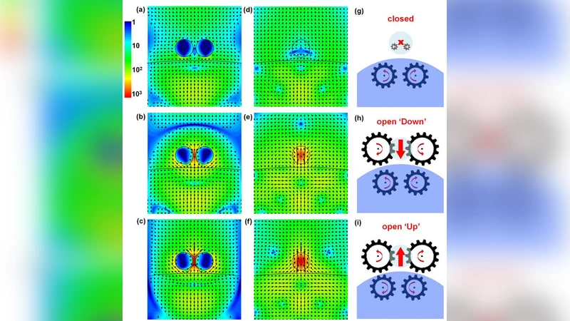
First, they demonstrate that a resonantly excited microcavity not only concentrates electromagnetic energy but also produces a dramatic spatial phase re‑distribution. Near the resonance frequency the dominant electric‑field component undergoes a 180° phase flip, and a multitude of phase singularities (points of zero field amplitude with undefined phase) appear, drift, and annihilate as the excitation wavelength is tuned. These singularities generate circulating power‑flow patterns—optical vortices—in the evanescent field surrounding the cavity. The position, number, and mutual coupling of these vortices can be precisely controlled by varying cavity parameters (size, refractive index) and the incident wavelength.
Second, the authors couple these vortex fields to noble‑metal nanoparticles (gold or silver). The rotating power‑flow around a vortex interacts strongly with the localized surface‑plasmon (LSP) modes of the particle, effectively opening or closing a nanoscale “gate” for plasmonic energy transfer. By adjusting the relative placement of the particle with respect to the vortex core, as well as the inter‑particle spacing, the authors show that the plasmonic transmission pathway can be switched on or off, redirected, or spectrally filtered—all without any external beam shaping or electrical bias.
Third, they outline a full on‑chip switching architecture. The high‑Q microcavity serves as a photon‑trapping element that recirculates light, providing narrow spectral selectivity while the vortex‑mediated gate controls the local flow of energy into downstream plasmonic elements. This configuration enables long‑range optical routing combined with sub‑diffraction confinement, as well as simultaneous spatial and spectral (de)multiplexing. Because the cavity dramatically modifies the local density of optical states (LDOS) at specific locations and frequencies, it also enhances light‑matter interaction with embedded quantum emitters (quantum dots, single molecules), opening pathways for deterministic photon‑emitter coupling in quantum circuits.
The paper’s key contributions are: (1) identification of the resonant phase‑reversal and vortex formation as a robust, tunable resource for nanoscale power‑flow control; (2) demonstration that these vortices can act as “nanogates” when interfaced with plasmonic nanoparticles, providing dynamic, reversible switching of plasmonic pathways; (3) a design framework showing how cavity geometry, material, and excitation wavelength can be engineered to achieve desired switching behavior without external modulators.
In conclusion, the authors argue that integrating high‑Q photonic elements into plasmonic networks offers a compact, low‑power, high‑speed alternative to existing active plasmonic devices. The approach promises scalable on‑chip implementation of optical logic, routing, and quantum‑information processing functions, and suggests future work on multi‑cavity vortex lattices, nonlinear material integration for optical logic gates, and experimental validation with realistic microdisk or microsphere resonators coupled to metallic nanostructures.
Comments & Academic Discussion
Loading comments...
Leave a Comment