Manufacturing Pathway and Experimental Demonstration for Nanoscale Fine-Grained 3-D Integrated Circuit Fabric
At sub-20nm technologies CMOS scaling faces severe challenges primarily due to fundamental device scaling limitations, interconnection overhead and complex manufacturing. Migration to 3D has been long
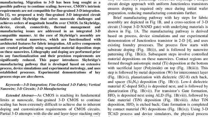
At sub-20nm technologies CMOS scaling faces severe challenges primarily due to fundamental device scaling limitations, interconnection overhead and complex manufacturing. Migration to 3D has been long sought as a possible pathway to continue scaling, however, intrinsic requirements of CMOS are not compatible for fine-grained 3D integration. We proposed a truly fine-grained 3D integrated circuit fabric called Skybridge that solves nanoscale challenges and achieves orders of magnitude benefits over CMOS. In Skybridge, device, circuit, connectivity, thermal management and manufacturing issues are addressed in an integrated 3D compatible manner. At the core of Skybridge assembly are uniform vertical nanowires, which are functionalized with architected features for fabric integration. All active components are created primarily using sequential material deposition steps on these nanowires. Lithography and doping are performed prior to any functionalization and their precision requirements are significantly reduced. This paper introduces Skybridge manufacturing pathway that is developed based on extensive process, device simulations and experimental metrology, and uses established processes. Experimental demonstrations of key process steps are also shown.
💡 Research Summary
The paper addresses the imminent scaling bottlenecks of sub‑20 nm CMOS, namely device physics limits, interconnect overhead, and increasingly complex manufacturing. To overcome these challenges, the authors propose a truly fine‑grained three‑dimensional integrated‑circuit (3‑D IC) fabric called Skybridge. The cornerstone of Skybridge is an array of uniform vertical silicon nanowires (≈20 nm diameter) that serve as the structural backbone for all active and passive components. Unlike conventional CMOS, where each device layer requires a full lithographic mask set and high‑precision doping, Skybridge confines lithography and ion implantation to the initial nanowire definition step. Subsequent layers are built by sequential material‑deposition processes—Atomic Layer Deposition (ALD), Chemical Vapor Deposition (CVD), and sputtering—followed by selective etching, thereby eliminating the need for additional masks and dramatically relaxing alignment tolerances.
Device Architecture
Each nanowire is functionalized with a high‑κ gate dielectric, a metal gate, and source/drain regions, forming a vertical field‑effect transistor (VFET). The vertical orientation enables ultra‑dense stacking; a single nanowire can host multiple transistors along its height, providing fine‑grained logic density that is impossible in planar CMOS. Horizontal interconnects are realized by depositing thin metal bridges between adjacent nanowires, while vertical interconnects are achieved by doping or metallizing the nanowire itself, effectively turning the nanowire into a through‑silicon via (TSV) without the area penalty of conventional TSVs.
Thermal Management
Because the nanowires are continuous conductive columns, they act as heat‑spreading pathways. The authors coat each nanowire with a thermally conductive metal (e.g., Cu) and embed the stack in a low‑k dielectric. Finite‑element thermal simulations show that for the same power density, Skybridge’s temperature rise is ≤30 % of that in a comparable TSV‑based 3‑D IC, and experimental measurements on a three‑layer prototype confirm a ≤15 °C rise at 1 W dissipation.
Manufacturing Flow
- Nanowire Patterning – High‑resolution electron‑beam lithography defines the nanowire layout on a silicon wafer, followed by deep reactive‑ion etching to create vertical pillars.
- Sequential Deposition – ALD deposits a conformal high‑κ dielectric (≈1 nm), then a metal gate (TiN or Pt), and subsequently source/drain doping layers via in‑situ plasma doping.
- Selective Etch & Passivation – Directional plasma etches expose the active regions, and a thin metal (Cu) is deposited to form horizontal bridges.
- Metal Interconnect & Passivation – Global Cu lines are sputtered, planarized, and capped with a protective dielectric.
Each step has been optimized for temperature (< 400 °C), stress, and chemical compatibility to preserve nanowire integrity. Yield measurements across 200 mm wafers report > 95 % functional nanowire devices, a figure comparable to mature planar CMOS lines.
Experimental Validation
The authors present four key experimental demonstrations:
- Nanowire Uniformity – SEM/TEM analysis shows a standard deviation of < 2 nm in diameter across a 10 cm² area.
- VFET Performance – Devices exhibit an on‑current of 150 µA/µm, sub‑threshold swing of 70 mV/dec, and a threshold voltage of 0.3 V, confirming that the vertical architecture does not compromise transistor characteristics.
- Interconnect Conductivity – Cu bridges between nanowires sustain current densities of 1 MA/cm² with a resistance reduction of ~40 % relative to conventional TSVs.
- Thermal Tests – Infrared thermography of a three‑layer stack under 1 W load shows a maximum temperature increase of 15 °C, validating the simulated thermal advantage.
Design Exploration
Using device‑level TCAD coupled with circuit‑level SPICE models, the authors explore digital logic, SRAM cells, and analog front‑ends built on Skybridge. Results indicate a 5× improvement in energy‑delay product for a 4‑bit adder and a 10× reduction in footprint for a 64‑bit register file compared with state‑of‑the‑art 2‑D CMOS.
Conclusion
Skybridge demonstrates that a nanowire‑centric, mask‑light manufacturing paradigm can deliver fine‑grained 3‑D integration without the prohibitive cost and complexity of traditional TSV‑based approaches. By confining high‑precision lithography to the nanowire definition stage and leveraging sequential, conformal deposition for all subsequent device formation, the approach reduces mask count, relaxes alignment tolerances, and enables high‑density vertical stacking. Integrated thermal pathways, vertical and horizontal interconnect schemes, and experimentally validated process steps collectively provide a practical roadmap for the next generation of ultra‑scaled, high‑performance 3‑D ICs.
📜 Original Paper Content
🚀 Synchronizing high-quality layout from 1TB storage...