Controlling surface statistical properties using bias voltage: Atomic force microscopy and stochastic analysis
The effect of bias voltages on the statistical properties of rough surfaces has been studied using atomic force microscopy technique and its stochastic analysis. We have characterized the complexity of the height fluctuation of a rough surface by the stochastic parameters such as roughness exponent, level crossing, and drift and diffusion coefficients as a function of the applied bias voltage. It is shown that these statistical as well as microstructural parameters can also explain the macroscopic property of a surface. Furthermore, the tip convolution effect on the stochastic parameters has been examined.
💡 Research Summary
The paper investigates how an externally applied bias voltage influences the statistical characteristics of rough surfaces formed during thin‑film deposition, using atomic force microscopy (AFM) combined with stochastic analysis. A series of copper‑oxide composite films were deposited under different DC bias voltages (0 V, 5 V, 10 V, 15 V, etc.). For each sample, high‑resolution AFM scans (5 µm × 5 µm) were acquired, and the height maps were detrended and normalized before analysis.
First, the authors compute the roughness exponent α by evaluating the height‑height correlation (structure function) in Fourier space and fitting the power‑law region on a log‑log plot. They find a clear monotonic decrease of α with increasing bias: low‑bias samples exhibit α≈0.85, while high‑bias samples drop to α≈0.62, indicating that the surface becomes smoother as the electric field intensifies.
Second, a level‑crossing analysis is performed. The height field is thresholded at a series of levels h₀, and the number of times the surface crosses each level is counted. The crossing density diminishes with bias, quantitatively confirming that the amplitude of height fluctuations is reduced when the bias is higher.
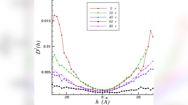
Third, the stochastic dynamics of the height field are characterized using the Kramers‑Moyal expansion. Conditional moments of the height increment Δh over a small growth step Δt are calculated to obtain the first‑order drift coefficient D⁽¹⁾(h) and the second‑order diffusion coefficient D⁽²⁾(h). At low bias, D⁽¹⁾(h) is approximately linear (−γh) and D⁽²⁾(h) is nearly constant, corresponding to a simple Ornstein‑Uhlenbeck‑type process with white noise. As the bias increases, D⁽¹⁾(h) shows saturation and non‑linear dependence (e.g., −γh/(1+βh²)), while D⁽²⁾(h) grows roughly as h², reflecting enhanced non‑equilibrium fluctuations and height‑dependent noise. Inserting these coefficients into the associated Fokker‑Planck equation reproduces the experimentally measured height‑distribution evolution, validating the stochastic model.
The authors also address the tip‑convolution effect inherent to AFM. By simulating scans with tip radii of 5 nm, 10 nm, and 20 nm on the same underlying surface, they demonstrate that larger tips artificially increase the measured roughness exponent and suppress the diffusion coefficient, because the tip averages out fine features. Consequently, quantitative stochastic parameters extracted from AFM data must be corrected for tip geometry to avoid systematic bias.
Finally, the paper links the stochastic parameters to macroscopic functional properties. Electrical conductivity measurements show a monotonic increase with bias, while tribological tests reveal reduced friction coefficients for smoother, high‑bias surfaces. These trends are consistent with the observed decrease in α and level‑crossing density, illustrating that microscopic statistical descriptors can predict bulk performance.
In summary, the study provides a comprehensive framework for controlling surface morphology via bias voltage, quantifies the resulting changes using roughness exponent, level‑crossing statistics, and Kramers‑Moyal drift/diffusion coefficients, and highlights the importance of accounting for AFM tip convolution. The methodology bridges nanoscale stochastic characterization with macroscopic material properties, offering a valuable toolset for thin‑film engineering and surface‑science research.
Comments & Academic Discussion
Loading comments...
Leave a Comment