Atomically thin group-V elemental films: theoretical investigations of antimonene allotropes
Group-V elemental monolayers including phosphorene are emerging as promising 2D materials with semiconducting electronic properties. Here, we present the results of first principles calculations on st
Group-V elemental monolayers including phosphorene are emerging as promising 2D materials with semiconducting electronic properties. Here, we present the results of first principles calculations on stability, mechanical and electronic properties of 2D antimony (Sb), antimonene. Our calculations show that free-standing {\alpha} and \b{eta} allotropes of antimonene are stable and semiconducting. The {\alpha}-Sb has a puckered structure with two atomic sub-layers and \b{eta}-Sb has a buckled hexagonal lattice. The calculated Raman spectra and STM images have distinct features thus facilitating characterization of both allotropes. The \b{eta}-Sb has nearly isotropic mechanical properties while {\alpha}-Sb shows strongly anisotropic characteristics. An indirect-direct band gap transition is expected with moderate tensile strains applied to the monolayers, which opens up the possibility of their applications in optoelectronics.
💡 Research Summary
The paper presents a comprehensive first‑principles investigation of two-dimensional antimony (antimonene) in its α (puckered) and β (buckled hexagonal) allotropes. Using density functional theory (DFT) with the PBE‑GGA functional and hybrid HSE06 corrections for electronic structure, the authors first optimize the crystal geometries and then assess dynamical stability through phonon dispersion calculations. Both α‑Sb and β‑Sb exhibit no imaginary phonon modes across the Brillouin zone, confirming that they are intrinsically stable as free‑standing monolayers.
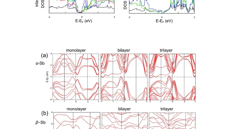
Structurally, α‑Sb resembles black phosphorus with a puckered configuration comprising two atomic sub‑layers separated by roughly 1.5 Å. Its lattice constants are anisotropic (a≈4.3 Å, b≈4.5 Å) and the internal bond angles deviate from the ideal 90°, leading to pronounced directional dependence. β‑Sb, by contrast, adopts a graphene‑like honeycomb lattice that is buckled out of plane by about 0.9 Å, with a single lattice constant a≈4.1 Å and six‑fold rotational symmetry.
Mechanical properties are extracted from the 2D elastic tensor Cij. β‑Sb shows near‑isotropic elasticity (C11≈C22≈45 N m⁻¹, C12≈15 N m⁻¹), yielding an average Young’s modulus of ~30 N m⁻¹ and a Poisson’s ratio around 0.2. α‑Sb is strongly anisotropic: C11≈55 N m⁻¹ along the puckering direction versus C22≈30 N m⁻¹ perpendicular to it, resulting in Young’s moduli that differ by a factor of ~1.8. This anisotropy translates into direction‑dependent strain tolerance, which is crucial for device engineering where specific mechanical responses are required.
Electronic band structures calculated with PBE place both allotropes in the semiconducting regime, with indirect gaps of ~0.9 eV (α‑Sb) and ~0.8 eV (β‑Sb). Hybrid functional corrections increase these gaps to roughly 1.2 eV and 1.1 eV, respectively. Importantly, the authors explore the effect of biaxial tensile strain up to 6 %. For α‑Sb, a modest ~4 % strain shifts the valence band maximum (VBM) and conduction band minimum (CBM) to the Γ point, effecting an indirect‑to‑direct gap transition and yielding a direct gap of about 1.0 eV. β‑Sb undergoes a similar transition at ~5 % strain, with the CBM moving from the X point to Γ. This strain‑induced band‑gap engineering suggests that antimonene can be tailored for optoelectronic applications such as strain‑gated transistors, photodetectors, and flexible photovoltaics.
Raman spectra are simulated to provide experimental fingerprints. α‑Sb exhibits two prominent Raman‑active modes: an Ag mode near 150 cm⁻¹ and a Bg mode around 210 cm⁻¹. β‑Sb shows a dominant Eg mode near 180 cm⁻¹. The distinct peak positions and intensities enable clear discrimination between the two phases using standard Raman spectroscopy. Scanning tunneling microscopy (STM) images are also generated: α‑Sb displays a pronounced height modulation reflecting its puckered topology, whereas β‑Sb presents a uniform honeycomb pattern consistent with its buckled hexagonal symmetry. These simulated images guide experimental identification and surface characterization.
In summary, the study establishes that both α‑ and β‑antimonene are dynamically stable, semiconducting 2D materials with markedly different mechanical anisotropies and strain‑responsive electronic properties. The ability to induce an indirect‑to‑direct band‑gap transition through moderate tensile strain opens a pathway for designing strain‑engineered devices. Moreover, the calculated Raman signatures and STM topographies provide practical tools for experimental verification. The findings position antimonene as a versatile platform for next‑generation nanoelectronics and optoelectronics, encouraging future experimental synthesis, heterostructure integration, and exploration of functional devices based on these novel 2D allotropes.
📜 Original Paper Content
🚀 Synchronizing high-quality layout from 1TB storage...