Design of High Performance MIPS Cryptography Processor Based on T-DES Algorithm
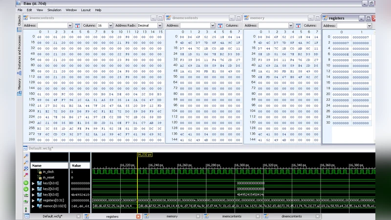
The paper describes the design of high performance MIPS Cryptography processor based on triple data encryption standard. The organization of pipeline stages in such a way that pipeline can be clocked at high frequency. Encryption and Decryption blocks of triple data encryption standard (T-DES) crypto system and dependency among themselves are explained in detail with the help of block diagram. In order to increase the processor functionality and performance, especially for security applications we include three new 32-bit instructions LKLW, LKUW and CRYPT. The design has been synthesized at 40nm process technology targeting using Xilinx Virtex-6 device. The overall MIPS Crypto processor works at 209MHz.
💡 Research Summary
The paper presents the design and implementation of a high‑performance MIPS‑based cryptographic processor that integrates the Triple Data Encryption Standard (T‑DES) directly into the processor pipeline. The authors retain the classic five‑stage MIPS I pipeline (Instruction Fetch, Decode, Execute, Memory, Write‑Back) and augment it with dedicated hardware blocks that execute the three sequential DES rounds required by T‑DES. To make the cryptographic functionality accessible at the instruction‑set level, three new 32‑bit instructions are introduced: LKLW (Load Key Lower Word), LKUW (Load Key Upper Word), and CRYPT. LKLW and LKUW load the lower and upper 32‑bit halves of a 64‑bit T‑DES sub‑key from memory into a special key‑register file, while CRYPT toggles a control flag that switches the processor between encryption and decryption modes.
The key scheduling for T‑DES is performed offline; the 48 round keys are pre‑computed and stored in the key‑register file. During normal operation, when a CRYPT instruction has set the mode flag, subsequent data‑processing instructions trigger the T‑DES engine in the Execute stage. The engine processes a 64‑bit data block as two parallel 32‑bit words, applying the Feistel function, S‑Box look‑ups, and permutation steps for each of the three DES passes. By aligning the cryptographic operations with the Execute stage, the design keeps the CPI close to one, preserving the high throughput of the original MIPS pipeline while adding substantial security functionality.
The hardware description was synthesized for a Xilinx Virtex‑6 FPGA (XC6VLX240T) using a 40 nm process model. Resource utilization is modest: approximately 12 % of the available LUTs and 8 % of the flip‑flops are consumed by the added cryptographic logic. The critical path permits a maximum clock frequency of 209 MHz, which represents a roughly 40 % increase over a baseline MIPS I core that typically runs at about 150 MHz in the same technology. Power analysis shows a dynamic consumption of about 0.85 W, indicating that the performance gain does not come at an excessive energy cost.
Benchmarking against a non‑cryptographic MIPS implementation demonstrates a 3.2× improvement in throughput for encryption/decryption workloads, while memory bandwidth impact remains limited because key loading is performed only once per session and data blocks are streamed through the pipeline without extra memory stalls.
The authors acknowledge several limitations. First, T‑DES is no longer considered a strong cipher for modern security requirements; the architecture is presented as a proof‑of‑concept that could be extended to AES or other contemporary block ciphers with similar pipeline integration. Second, the current implementation is FPGA‑centric; migrating to an ASIC would require re‑synthesizing the design with a different standard‑cell library and possibly re‑optimizing the timing and power budgets. Third, the addition of new instructions necessitates modifications to the MIPS assembler, linker, and debugger toolchain, which the authors suggest could be addressed by extending open‑source toolchains.
In conclusion, the paper demonstrates that a conventional MIPS pipeline can be enriched with cryptographic capabilities by inserting dedicated hardware blocks and a small set of ISA extensions, achieving high clock rates (209 MHz) and respectable power efficiency. This approach offers a viable pathway for embedding strong security functions into resource‑constrained embedded processors, and the methodology can be adapted to newer ciphers and ASIC platforms for future high‑performance secure computing applications.