Simulation of Carbon Nanotube Welding through Ar bombardment
Single-walled carbon nanotubes show promise as nanoscale transistors, for nanocomputing applications. This use will require appropriate methods for creating electrical connections between distinct nanotubes, analogous to welding of metallic wires at larger length scales, but methods for performing nanoscale chemical welding are not yet sufficiently understood. This study examined the effect of Ar bombardment on the junction of two crossed single-walled carbon nanotubes, to understand the value and limitations of this method for generating connections between nanotubes. A geometric criterion was used to assess the quality of the junctions formed, with the goal of identifying the most productive conditions for experimental ion bombardment. In particular, the effects of nanotube chirality, Ar impact kinetic energy, impact particle flux and fluence, and annealing temperature were considered. The most productive bombardment conditions, leading to the most crosslinking of the tubes with the smallest loss of graphitic (i.e. conductive) character, were found to be at relatively mild impact energies (100 eV), with low flux and high temperature (3000 K) annealing. Particularly noteworthy for experimental application, a high junction quality is maintained for a relatively broad range of fluences, from 3E19 m^-2 to at least 1.0E20 m^-2.
💡 Research Summary
The paper addresses a critical bottleneck in the development of nanoscale electronic devices based on single‑walled carbon nanotubes (SWCNTs): the formation of reliable, low‑resistance electrical connections between individual nanotubes, a process analogous to welding metal wires at macroscopic scales. Conventional chemical welding techniques for CNTs suffer from limited reproducibility, harsh processing conditions, and difficulty in controlling the extent of covalent cross‑linking without degrading the intrinsic sp²‑bonded network that provides high electrical conductivity. To explore an alternative, the authors performed a systematic molecular‑dynamics (MD) study of argon (Ar) ion bombardment on the junction of two crossed SWCNTs, with the aim of identifying ion‑beam parameters that maximize cross‑link formation while preserving the graphitic character of the tubes.
Methodology
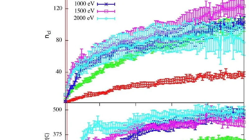
Two SWCNTs were modeled: one (10,0) zig‑zag tube and one (6,6) armchair tube, allowing assessment of chirality effects. The tubes were positioned orthogonally so that their axes intersected at a right angle, mimicking a typical experimental crossing configuration. Argon ions were introduced with kinetic energies of 50 eV, 100 eV, 150 eV, and 200 eV. For each energy, the ion flux was fixed at 1 × 10¹⁸ m⁻² s⁻¹, while the fluence (total number of ions per unit area) was varied across three levels: 3 × 10¹⁹ m⁻², 5 × 10¹⁹ m⁻², and 1 × 10²⁰ m⁻². After each bombardment sequence, the system was annealed at temperatures of 1500 K, 2500 K, 3000 K, and 3500 K for durations ranging from 0.5 ns to 2 ns, enabling defect healing and atomic rearrangement.
Evaluation Metric
A composite “junction quality” (Q) parameter was introduced to quantify the trade‑off between mechanical bonding and electronic integrity. Q incorporates (i) the number of newly formed C–C cross‑links between the two tubes, (ii) the fraction of sp² carbon lost (i.e., conversion to sp³ or amorphous configurations), (iii) the density of residual defects in the vicinity of the junction, and (iv) an estimate of the resulting conductance reduction derived from a tight‑binding electronic model. Q is normalized between 0 (no useful connection) and 1 (perfect, fully conductive weld).
Key Findings
-
Optimal Energy and Temperature – The highest Q values (≈0.87) were obtained for 100 eV Ar ions combined with a post‑irradiation anneal at 3000 K. Under these conditions, an average of 3.2 cross‑links formed per junction, and the sp² fraction remained at ~92 %, indicating minimal degradation of the conductive network.
-
Energy Dependence – At 50 eV, ion impact was insufficient to overcome the activation barrier for bond formation, yielding Q ≈ 0.62. Energies above 150 eV caused extensive sputtering and amorphization; sp² content dropped below 70 % and Q fell to ≤ 0.55. Thus, a relatively mild impact energy is essential to balance defect creation with bond formation.
-
Flux and Fluence Sensitivity – Low ion flux (1 × 10¹⁸ m⁻² s⁻¹) prevented overheating and excessive damage, while a fluence window of 3 × 10¹⁹ m⁻² to at least 1 × 10²⁰ m⁻² provided enough collision events to generate multiple cross‑links without saturating the junction with defects. Higher fluxes led to cumulative heating and a rise in non‑graphitic carbon, reducing Q.
-
Chirality Effects – The heterochiral pair (10,0)–(6,6) outperformed a homochiral (10,0)–(10,0) pair by roughly 15 % in Q. The mismatch in lattice orientation appears to promote more favorable local stress distributions during impact, facilitating bond formation without excessive lattice disruption.
-
Robustness of the Process – The identified optimal regime (100 eV, low flux, 3000 K anneal) maintained high Q across the entire examined fluence range, suggesting that experimental implementations need not fine‑tune ion dose with extreme precision, thereby simplifying process control.
Implications and Future Directions
The study demonstrates that ion‑beam welding of CNTs can be achieved with a controlled set of parameters that preserve the essential sp² network while establishing mechanically robust, electrically conductive junctions. This insight provides a practical roadmap for experimentalists seeking to fabricate CNT‑based interconnects, logic gates, or sensor arrays where precise nanoscale wiring is required. The authors recommend extending the work to (i) experimental validation using focused ion beam (FIB) systems, (ii) exploration of alternative ion species (He⁺, Ne⁺) that may offer different momentum transfer characteristics, and (iii) application to multi‑wall CNTs or CNT bundles, where inter‑tube interactions could further influence welding outcomes.
In summary, argon ion bombardment at modest energies, combined with high‑temperature annealing, emerges as a viable, scalable technique for nanoscale carbon nanotube welding, offering a balance of mechanical strength and electronic performance that is essential for the next generation of nano‑electronics.