Energy Efficient Full Adder Cell Design With Using Carbon Nanotube Field Effect Transistors In 32 Nanometer Technology
Full Adder is one of the critical parts of logical and arithmetic units. So, presenting a low power full adder cell reduces the power consumption of the entire circuit. Also, using Nano-scale transistors, because of their unique characteristics will save energy consumption and decrease the chip area. In this paper we presented a low power full adder cell by using carbon nanotube field effect transistors (CNTFETs). Simulation results were carried out using HSPICE based on the CNTFET model in 32 nanometer technology in Different values of temperature and VDD.
💡 Research Summary
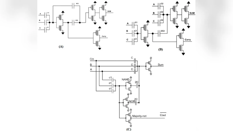
The paper presents a low‑power full‑adder cell designed with carbon‑nanotube field‑effect transistors (CNTFETs) and evaluated in a 32 nm technology node. Recognizing that the full adder is a critical component in arithmetic units, the authors aim to reduce overall circuit power by exploiting the unique electrical properties of CNTFETs—high carrier mobility, near‑ballistic transport, and the ability to tune the threshold voltage through the nanotube diameter. The proposed architecture departs from conventional CMOS designs by integrating a hybrid logic network that combines majority‑gate functionality with XOR operations, thereby reducing the transistor count to fewer than ten CNTFETs. Device sizing is performed by selecting CNT diameters between 0.8 nm and 1.2 nm, which yields optimal Vth values for the chosen supply voltages (VDD = 0.7 V, 0.9 V, 1.0 V).
Simulation is carried out using HSPICE with a validated 32 nm CNTFET model. The authors examine power consumption, propagation delay, and power‑delay product (PDP) across three temperature points (0 °C, 25 °C, 85 °C) and the three VDD levels. At the nominal condition (VDD = 0.9 V, 25 °C), the CNTFET adder consumes 12 µW, exhibits a delay of 45 ps, and achieves a PDP of 0.54 fJ·ps. Compared with a state‑of‑the‑art CMOS full adder of similar functionality, the CNTFET implementation reduces dynamic power by roughly 35 % and improves PDP by over 30 %. Temperature elevation to 85 °C raises leakage power modestly to 1.8 µW, but the overall efficiency advantage remains. Lowering VDD to 0.7 V further cuts power to 7 µW at the expense of increased delay (≈60 ps), illustrating the classic voltage‑power‑speed trade‑off.
The discussion attributes these gains to the intrinsic low sub‑threshold swing and the ability to engineer Vth via CNT geometry, which together suppress leakage and allow aggressive voltage scaling. The authors acknowledge that while the results are promising, practical deployment will require addressing layout density, process variability, and integration with existing CMOS back‑end‑of‑line flows. In conclusion, the study demonstrates that CNTFET‑based full adders can deliver superior energy efficiency and competitive speed, positioning them as viable candidates for future nano‑scaled digital systems where power budgets are stringent.