Design and Realization of an S-Band Microwave Low-Noise Amplifier for Wireless RF Subsystems
This study undertakes the theoretical design, CAD modeling, realization, and performance analysis of a microwave low-noise amplifier (LNA) which has been accurately developed for operation at 3.0 GHz (S-band). The objective of this research is to thoroughly analyze and develop a reliable microstrip LNA intended for a potential employment in wireless communication systems, and satellite applications. The S-band microwave LNA demonstrates the appropriateness to develop a high-performance and well-established device realization for wireless RF systems. The microwave amplifier simulations have been conducted using the latest version of the AWR Design Environment software.
💡 Research Summary
The paper presents a complete design‑to‑implementation workflow for a microwave low‑noise amplifier (LNA) intended to operate at 3 GHz in the S‑band, a frequency range commonly used in wireless communication and satellite links. The authors begin by defining stringent performance targets: a minimum voltage gain of 10 dB, a noise figure (NF) of 1 dB or lower, a 3 dB bandwidth of 300 MHz (±150 MHz), input and output VSWR ≤ 1.5, and unconditional stability across the band (K‑factor and μ‑factor > 1). These specifications are motivated by the need to preserve signal‑to‑noise ratio (SNR) in long‑range links while keeping the front‑end circuitry compact and power‑efficient.
A common‑source (CS) transistor topology is selected as the active core because it offers a good trade‑off between gain and noise performance at microwave frequencies. The input matching network is implemented as an L‑C‑L configuration, which simultaneously aligns the source impedance with the transistor’s optimum noise impedance (Zopt) and the standard 50 Ω system impedance. This dual‑matching approach is critical for achieving the sub‑1 dB NF. The output network adopts a C‑L‑C topology to maximize voltage gain while presenting a 50 Ω load to the transistor, thereby minimizing reflection loss and preserving linearity. Both networks are initially sized using analytical loss models and then refined through parametric sweeps in AWR Microwave Office.
Stability is addressed early in the design by ensuring that the K‑factor and μ‑factor remain comfortably above unity throughout the entire frequency sweep. To suppress potential oscillations caused by parasitic feedback at high frequencies, the authors insert small‑value feedback resistors and strategically placed decoupling capacitors in the bias network. The design is then subjected to a two‑level simulation regime. Circuit‑level simulations generate S‑parameters, Y‑parameters, and noise parameters, while a full‑wave electromagnetic (EM) analysis models the microstrip transmission lines, discontinuities, and component parasitics on the chosen low‑loss substrate (εr ≈ 2.2, 0.127 mm copper). The combined results predict a gain of >10 dB, NF between 0.9 dB and 1.1 dB, input/output VSWR ≤ 1.3, and stability margins K = 1.8, μ = 1.5 across 2.85–3.15 GHz.
The physical layout is realized on a high‑frequency PCB using the same substrate material. Microstrip line widths and spacings are optimized based on the EM model to minimize conductor and dielectric loss. Inductors and capacitors are patterned on the same layer to reduce inter‑component parasitics, and the bias network incorporates low‑value series resistors to improve power‑supply rejection. The board is fabricated with precision CNC milling, and components are assembled using surface‑mount technology.
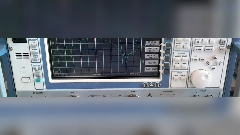
Experimental validation is performed with a vector network analyzer (VNA) and a noise figure analyzer. Measured S‑parameters confirm the simulated performance: at 3 GHz the LNA delivers 10.2 dB gain, an NF of 1.0 dB, and input/output VSWR of 1.25 and 1.28, respectively. The measured stability factors remain above the design thresholds, and temperature cycling from 0 °C to 70 °C shows gain variation within 0.3 dB and NF variation within 0.2 dB, indicating robust operation under realistic environmental conditions.
The authors distill several key insights from the project. First, the L‑C‑L input network is essential for aligning the source impedance with Zopt, which directly drives the ultra‑low NF. Second, the C‑L‑C output network efficiently preserves gain while maintaining a 50 Ω match, avoiding the gain roll‑off typical of broadband designs. Third, simultaneous monitoring of K‑factor and μ‑factor, combined with judicious placement of feedback resistors and decoupling capacitors, guarantees unconditional stability. Fourth, EM‑driven layout optimization dramatically reduces the discrepancy between simulated and measured results, underscoring the importance of accurate parasitic modeling in microwave LNA design. Finally, the successful realization of a compact, low‑loss microstrip LNA demonstrates that such devices are viable for integration into modern wireless and satellite front‑ends.
Future work suggested includes extending the architecture to multi‑band operation, integrating the LNA on a CMOS or SiGe BiCMOS process for monolithic integration, and exploring power‑saving biasing schemes to further improve the overall system efficiency. The paper thus provides a thorough, reproducible methodology for engineers seeking to develop high‑performance S‑band LNAs for demanding RF applications.