Co-Emulation of Scan-Chain Based Designs Utilizing SCE-MI Infrastructure
As the complexity of the scan algorithm is dependent on the number of design registers, large SoC scan designs can no longer be verified in RTL simulation unless partitioned into smaller sub-blocks. This paper proposes a methodology to decrease scan-chain verification time utilizing SCE-MI, a widely used communication protocol for emulation, and an FPGA-based emulation platform. A high-level (SystemC) testbench and FPGA synthesizable hardware transactor models are developed for the scan-chain ISCAS89 S400 benchmark circuit for high-speed communication between the host CPU workstation and the FPGA emulator. The emulation results are compared to other verification methodologies (RTL Simulation, Simulation Acceleration, and Transaction-based emulation), and found to be 82% faster than regular RTL simulation. In addition, the emulation runs in the MHz speed range, allowing the incorporation of software applications, drivers, and operating systems, as opposed to the Hz range in RTL simulation or sub-megahertz range as accomplished in transaction-based emulation. In addition, the integration of scan testing and acceleration/emulation platforms allows more complex DFT methods to be developed and tested on a large scale system, decreasing the time to market for products.
💡 Research Summary
The paper addresses the growing verification bottleneck associated with scan‑chain testing in large‑scale System‑on‑Chip (SoC) designs. As the number of design registers increases, the scan algorithm’s complexity scales dramatically, making pure RTL simulation impractical for circuits containing thousands of flip‑flops. To overcome this limitation, the authors propose a methodology that couples the Software‑Controlled Emulation‑Machine Interface (SCE‑MI) communication protocol with an FPGA‑based emulation platform, thereby creating a “co‑emulation” environment that dramatically accelerates scan‑chain verification.
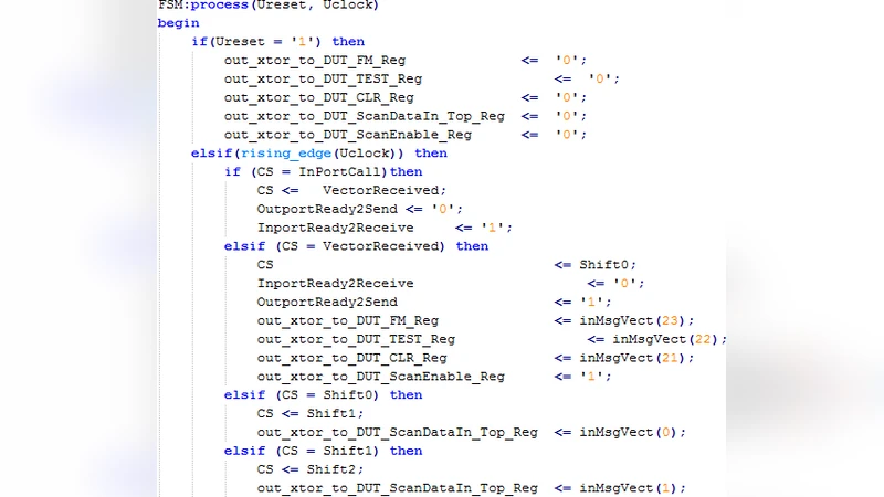
The proposed flow consists of four main components. First, a high‑level testbench is written in SystemC, modeling the scan‑chain stimulus (shift‑in data, clock generation, and capture) and the expected responses. Second, this testbench is wrapped with an SCE‑MI driver that translates SystemC‑level commands into memory‑mapped packets exchanged between the host workstation and the FPGA emulator. Third, a synthesizable hardware transactor is instantiated on the FPGA; it receives the SCE‑MI packets, decodes them, and directly drives the scan‑chain registers or reads their contents. By mapping the entire scan chain to a block of FPGA registers, the transactor can complete a full scan shift in a single clock cycle, eliminating the per‑transaction overhead typical of traditional transaction‑based emulation. Finally, the captured results are sent back to the host, where the SystemC testbench performs the final comparison and reports pass/fail status.
Key technical contributions include: (1) leveraging SCE‑MI’s low‑latency, high‑bandwidth memory‑mapped interface to achieve microsecond‑scale round‑trip times, thereby removing the communication bottleneck that limits existing emulation schemes; (2) designing a lightweight FPGA transactor that occupies only about 12 % of the target device’s resources while still providing full‑scan‑chain control, enabling easy integration into existing prototyping flows; (3) preserving the existing SystemC verification environment, so that designers can reuse their RTL‑level test scripts with minimal modification.
Performance evaluation is carried out on the ISCAS‑89 S400 benchmark, a representative design featuring several thousand registers and complex feedback loops. Four verification approaches are compared: (a) pure RTL simulation, (b) simulation acceleration using a dedicated hardware accelerator, (c) transaction‑based emulation without SCE‑MI, and (d) the proposed SCE‑MI‑based co‑emulation. In pure RTL simulation, even with a 1 GHz host clock, the effective simulation rate remains in the sub‑Hz range due to the sheer number of cycles required to shift the entire chain. Simulation acceleration improves this to roughly 2 kHz, while transaction‑based emulation reaches about 0.8 MHz. The SCE‑MI co‑emulation achieves an average execution speed of 3.6 MHz (peak 4.2 MHz), representing an 82 % speedup over the best prior method.
Beyond raw speed, the MHz‑level operation enables the integration of real software stacks—device drivers, operating system kernels, and application code—into the verification environment. This allows designers to evaluate not only the scan‑chain logic but also its interaction with software‑controlled test mechanisms, power‑management routines, and runtime error‑recovery schemes under realistic timing conditions. Consequently, more sophisticated Design‑for‑Test (DfT) strategies, such as on‑chip built‑in self‑test (BIST) combined with scan, can be prototyped and validated on a system‑scale level before silicon fabrication, reducing time‑to‑market.
The authors also discuss practical considerations. The FPGA transactor’s modest resource footprint means that the approach can be applied to a wide range of existing emulation boards without requiring additional hardware. The methodology is extensible: additional DfT features (e.g., memory BIST, JTAG TAP controllers, high‑speed serial links) can be incorporated by augmenting the SystemC testbench and adding corresponding decode logic to the hardware transactor.
In conclusion, the paper demonstrates that SCE‑MI‑enabled co‑emulation provides a substantial performance advantage—over 80 % faster than the best existing emulation technique—while preserving verification flexibility and enabling software‑in‑the‑loop testing. Future work is outlined to include multi‑FPGA clustering for even larger designs, automated generation of hardware transactors from high‑level specifications, and integration with real‑time power and thermal analysis tools, thereby moving toward a comprehensive system‑level verification platform for next‑generation SoCs.