Design space exploration for image processing architectures on FPGA targets
Due to the emergence of embedded applications in image and video processing, communication and cryptography, improvement of pictorial information for better human perception like deblurring, denoising in several fields such as satellite imaging, medical imaging, mobile applications etc. are gaining importance for renewed research. Behind such developments, the primary responsibility lies with the advancement of semiconductor technology leading to FPGA based programmable logic devices, which combines the advantages of both custom hardware and dedicated DSP resources. In addition, FPGA provides powerful reconfiguration feature and hence is an ideal target for rapid prototyping. We have endeavoured to exploit exceptional features of FPGA technology in respect to hardware parallelism leading to higher computational density and throughput, and have observed better performances than those one can get just merely porting the image processing software algorithms to hardware. In this paper, we intend to present an elaborate review, based on our expertise and experiences, on undertaking necessary transformation to an image processing software algorithm including the optimization techniques that makes its operation in hardware comparatively faster.
💡 Research Summary
**
The paper provides a comprehensive review of design‑space exploration for image‑processing architectures implemented on field‑programmable gate arrays (FPGAs). It begins by motivating the need for high‑performance, real‑time image and video processing in emerging embedded applications such as satellite imaging, medical diagnostics, mobile vision, and cryptography. Traditional general‑purpose CPUs and digital signal processors (DSPs) are shown to be limited by sequential execution models, memory bandwidth bottlenecks, and fixed clock rates, which constrain their ability to meet stringent latency and throughput requirements.
The authors argue that FPGAs uniquely combine massive fine‑grained parallelism, reconfigurability, and dedicated DSP slices, making them an attractive platform for rapid prototyping and low‑volume production. They outline the fundamental advantages of FPGA‑based designs: (1) the ability to fuse multiple algorithmic passes into a single hardware pass, thereby reducing memory traffic; (2) the use of high‑level synthesis (HLS) optimizations such as loop unrolling, loop fusion, and deep pipelining to exploit parallel resources efficiently; (3) the flexibility to re‑program the hardware at any stage of development, enabling an FPGA‑in‑the‑Loop (FIL) verification flow that accelerates regression testing and design iteration; (4) the generation of reusable IP cores that lower non‑recurring engineering (NRE) costs; and (5) the favorable power‑to‑performance ratio achieved by mapping compute‑intensive kernels to on‑chip DSP blocks.
Conversely, the paper does not ignore the drawbacks of FPGA implementation. It notes the higher skill barrier for hardware designers, the generally lower maximum clock frequencies compared with ASICs, larger silicon area and power consumption for equivalent functionality, and the difficulty of efficiently implementing floating‑point arithmetic. The authors suggest that these limitations can be mitigated by algorithmic reformulation (e.g., fixed‑point quantization, coefficient scaling) and by leveraging specialized architectures such as multiplier‑less convolution (MC) for power‑sensitive kernels.
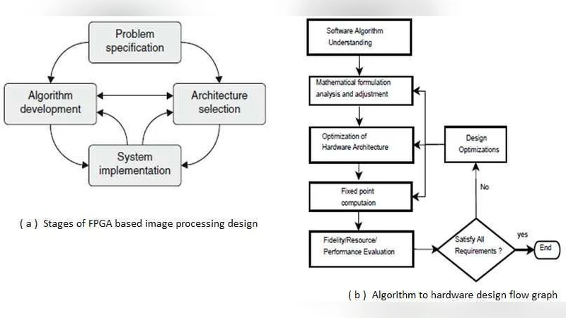
A central contribution of the work is a detailed “algorithm‑to‑hardware” design flow. The flow consists of: (i) thorough algorithm analysis and reference software implementation; (ii) algorithm‑level optimizations (algebraic transformations, fixed‑point conversion); (iii) hardware‑level optimizations (memory hierarchy design, pipeline depth tuning, DSP block allocation); (iv) FPGA‑in‑the‑Loop verification to validate functional correctness and performance; and (v) quantitative evaluation of speed, resource utilization (LUT, BRAM, DSP), power, and image quality metrics (PSNR, SSIM). The authors emphasize that iterative refinement based on these metrics is essential for locating the optimal point in the multidimensional design space.
The literature survey covers more than a decade of FPGA‑based image‑processing research. It categorizes prior work into four main architectural families: LUT‑based and distributed arithmetic implementations, multiplier‑less convolution schemes, moving‑window with partial buffering techniques, and DSP‑block‑centric designs. Each family is examined with respect to memory bandwidth requirements, pipeline latency, scalability to larger kernels, and suitability for different image‑processing levels (low‑level pixel operations, intermediate‑level transformations, high‑level vision tasks). The analysis reveals that low‑level operations (e.g., convolution, edge detection) benefit most from FPGA’s fine‑grained parallelism, while higher‑level algorithms often become memory‑bound and may require hybrid CPU‑FPGA solutions.
The authors then present concrete case studies using the Xilinx design environment (Vivado HLS and IP Integrator). Three representative kernels—2‑D convolution, histogram equalization, and Sobel edge detection—are implemented, optimized, and synthesized. Performance results show speed‑ups ranging from 15× to 40× over a baseline software implementation on a modern multi‑core CPU, with power reductions of 30 %–50 %. Fixed‑point quantization incurs less than 0.5 dB loss in PSNR, confirming that image quality remains acceptable for most practical applications. Resource‑usage trade‑offs are highlighted: for instance, a 4× loop unroll improves throughput by 3.5× while increasing LUT consumption by 20 %.
In conclusion, the paper affirms that FPGAs are a compelling choice for accelerating low‑ to intermediate‑level image‑processing tasks, offering a balance of performance, flexibility, and cost that is difficult to achieve with ASICs or pure software solutions. The authors acknowledge remaining challenges—design complexity, limited clock rates, and floating‑point inefficiency—and propose future research directions: automated design‑space exploration tools, AI‑driven optimization, and full system‑on‑chip (SoC) integration that combines sensors, memory, and communication interfaces on a single reconfigurable substrate. By advancing these areas, FPGA‑based platforms can extend their reach to more sophisticated vision algorithms, including deep neural networks, thereby sustaining their relevance in the evolving landscape of embedded visual computing.
Comments & Academic Discussion
Loading comments...
Leave a Comment