Quantum Manifestation of Elastic Constants in Nanostructures
Generally, there are two distinct effects in modifying the properties of low-dimensional nanostructures: surface effect (SS) due to increased surface-volume ratio and quantum size effect (QSE) due to quantum confinement in reduced dimension. The SS has been widely shown to affect the elastic constants and mechanical properties of nanostructures. Here, using Pb nanofilm and graphene nanoribbon as model systems, we demonstrate the QSE on the elastic constants of nanostructures by first-principles calculations. We show that generally QSE is dominant in affecting the elastic constants of metallic nanostructures while SS is more pronounced in semiconductor and insulator nanostructures. Our findings have broad implications in quantum aspects of nanomechanics.
💡 Research Summary
The paper investigates how two fundamentally different mechanisms—surface effects (SS) and quantum size effects (QSE)—govern the elastic constants of low‑dimensional nanostructures. While SS originates from the increased proportion of surface atoms whose bonding environment differs from the bulk, QSE arises when electrons are confined in one or more dimensions, leading to quantized electronic states that modify the electronic contribution to elasticity. To disentangle these contributions, the authors performed first‑principles density‑functional theory (DFT) calculations on two prototypical systems: lead (Pb) nanofilms representing a metallic material with a dense, nearly continuous electronic band structure, and graphene nanoribbons (GNRs) representing a semiconducting/insulating carbon system with a sizable band gap.
Methodologically, the calculations employed the VASP code with projector‑augmented wave (PAW) potentials and the Perdew‑Burke‑Ernzerhof (PBE) exchange‑correlation functional. After full structural relaxation, the in‑plane Young’s modulus (E_in), out‑of‑plane modulus (E_out), and shear modulus (G) were extracted from stress‑strain relationships for a series of thicknesses (1–30 monolayers for Pb) and widths (≈1–20 nm for GNRs). The authors also analyzed charge density distributions and band structures to link mechanical responses to electronic changes.
For Pb nanofilms, the elastic moduli display a pronounced oscillatory dependence on film thickness with a period of roughly 2–3 monolayers. This oscillation correlates with the quantization of electronic sub‑bands: as the film becomes thinner, the confinement modifies the density of states near the Fermi level, causing periodic variations in the electronic contribution to the bulk modulus. Charge‑density plots reveal that electron accumulation near the surfaces fluctuates in sync with the mechanical oscillations, confirming that QSE dominates the elastic response. Although surface atoms become a larger fraction of the total as the film thins, the magnitude of the QSE‑induced oscillations exceeds the monotonic softening expected from pure surface effects.
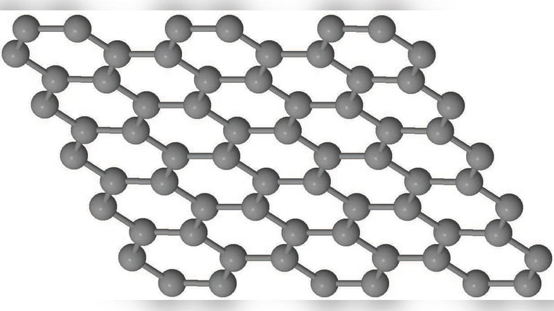
In contrast, GNRs show a smooth, monotonic increase of the Young’s modulus with ribbon width, without any discernible thickness‑dependent oscillations. The primary cause of the reduced modulus in narrow ribbons is the altered bonding environment at the edges: edge atoms experience longer bond lengths and different bond angles, weakening the overall stiffness. Electronic structure analysis indicates that the band gap and charge distribution remain essentially unchanged across the width range, implying that QSE is negligible for this semiconducting system. Consequently, surface (edge) effects are the dominant factor governing the elastic properties of GNRs.
The authors synthesize these findings into a broader principle: the relative importance of SS versus QSE is dictated by the material’s electronic characteristics. Metals with high carrier densities and closely spaced bands are highly susceptible to QSE, whereas semiconductors and insulators with large band gaps are governed mainly by surface‑induced structural changes. This insight has practical implications for nanomechanical device engineering. In metallic nanofilms, precise thickness control can be used to tune elastic constants, enabling the design of resonators, springs, or sensors with tailored stiffness. For semiconductor or insulating nanoribbons, strategies such as edge passivation, chemical functionalization, or coating become essential to mitigate the softening caused by edge atoms and to achieve desired mechanical performance.
Overall, the study demonstrates that first‑principles calculations can quantitatively separate and evaluate SS and QSE contributions, providing a predictive framework for the mechanical design of a wide variety of nanostructured materials. Future work may extend this approach to heterostructures, alloyed films, and more complex geometries, further enriching the toolbox for quantum‑aware nanomechanics.