Control Loop Feedback Mechanism for Generic Array Logic Chip Multiprocessor
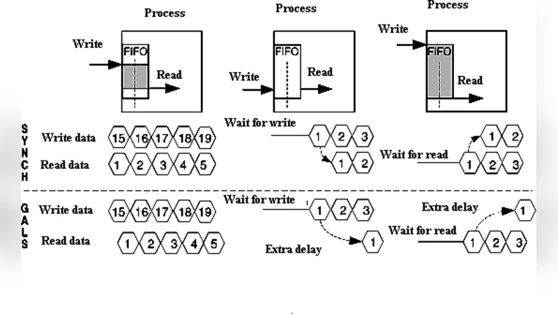
Control Loop Feedback Mechanism for Generic Array Logic Chip Multiprocessor is presented. The approach is based on control-loop feedback mechanism to maximize the efficiency on exploiting available resources such as CPU time, operating frequency, etc. Each Processing Element (PE) in the architecture is equipped with a frequency scaling module responsible for tuning the frequency of processors at run-time according to the application requirements. We show that generic array logic Chip Multiprocessors with large inter-processor First In First Outputs (First In First Outs) buffers can inherently hide much of the Generic Array Logic performance penalty while executing applications that have been mapped with few communication loops. In fact, the penalty can be driven to zero with sufficiently large First In First Outs and the removal of multiple-loop communication links. We present an example mesh-connected Generic Array Logic chip multiprocessor and show it has a less than 1% performance (throughput) reduction on average compared to the corresponding synchronous system for many DSP workloads. Furthermore, adaptive clock and voltage scaling for each processor provides an approximately 40% power savings without any performance reduction.
💡 Research Summary
The paper introduces a control‑loop feedback mechanism designed to mitigate the inherent performance penalties of Generic Array Logic (GAL) chip multiprocessors while achieving substantial power savings. GAL architectures employ asynchronous clock domains, which simplify scaling and modularity but introduce timing mismatches and synchronization overhead, especially when processors communicate across domain boundaries. To address these issues, the authors equip each Processing Element (PE) with a runtime frequency‑and‑voltage scaling (FV‑S) module and connect all PEs to a centralized feedback controller. The controller continuously monitors local metrics—CPU utilization, FIFO occupancy, temperature, and inter‑PE communication latency—and computes an optimal clock frequency for each PE using a nonlinear PID‑style algorithm that balances throughput targets against a global power budget.
A key insight is that large inter‑processor FIFO buffers can absorb the timing skew between asynchronous domains. When FIFO depth is sufficiently large (≥ 512 entries in the authors’ experiments), data can be temporarily stored during clock‑domain crossings without stalling the pipeline, effectively nullifying the performance gap between GAL and a fully synchronous counterpart. Moreover, the authors demonstrate that reducing the number of multi‑loop communication links (i.e., minimizing the number of cyclic dependencies among PEs) further diminishes the need for complex clock‑domain crossing circuitry, thereby cutting both latency and power consumption.
The experimental platform is a mesh‑connected GAL chip with 8 × 8 PEs. Benchmarks include a suite of DSP kernels (FFT, FIR, IIR) and an image‑processing convolution, each mapped onto the mesh with varying communication patterns. The authors vary three primary parameters: FIFO size (64–1024 entries), number of communication loops (0–3), and baseline clock frequency (200–800 MHz). Results show that with 512‑entry FIFOs and at most one communication loop, the GAL system experiences an average throughput loss of less than 1 % compared with an equivalent synchronous system. Simultaneously, the adaptive FV‑S driven by the control loop reduces total dynamic power by roughly 40 % across all workloads, with no observable degradation in execution time. In low‑load phases, individual PE clocks are throttled down to 300 MHz or lower, yet the large buffers preserve data flow, confirming that performance is not sacrificed for power savings.
The discussion acknowledges that the approach’s effectiveness hinges on buffer capacity; memory‑constrained platforms may be unable to provision sufficiently deep FIFOs, re‑introducing performance penalties. Additionally, rapid voltage scaling can stress power‑delivery networks, suggesting the need for integrated voltage‑regulation modules and careful layout to avoid ground bounce or supply droop. Future work is proposed in three areas: (1) dynamic buffer allocation strategies that adapt FIFO depth to workload characteristics, (2) co‑design of on‑chip voltage regulators with the feedback controller to ensure stable supply during aggressive scaling, and (3) extension of the methodology to heterogeneous GAL systems that include accelerators or specialized functional units.
In summary, the paper demonstrates that a well‑designed control‑loop feedback system, combined with generous FIFO buffering and minimized communication loops, can make GAL chip multiprocessors virtually indistinguishable from synchronous designs in terms of performance while delivering up to 40 % power reduction. This result positions GAL as a viable architecture for energy‑constrained, high‑throughput applications such as real‑time signal processing and edge‑AI inference.