Through Silicon Via Aware Design Planning for Thermally Efficient 3-D Integrated Circuits
3-D integrated circuits (3-D ICs) offer performance advantages due to their increased bandwidth and reduced wire-length enabled by through-silicon-via structures (TSVs). Traditionally TSVs have been c
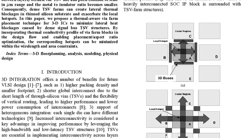
3-D integrated circuits (3-D ICs) offer performance advantages due to their increased bandwidth and reduced wire-length enabled by through-silicon-via structures (TSVs). Traditionally TSVs have been considered to improve the thermal conductivity in the vertical direction. However, the lateral thermal blockage effect becomes increasingly important for TSV via farms (a cluster of TSV vias used for signal bus connections between layers) because the TSV size and pitch continue to scale in μm range and the metal to insulator ratio becomes smaller. Consequently, dense TSV farms can create lateral thermal blockages in thinned silicon substrate and exacerbate the local hotspots. In this paper, we propose a thermal-aware via farm placement technique for 3-D ICs to minimize lateral heat blockages caused by dense signal bus TSV structures. By incorporating thermal conductivity profile of via farm blocks in the design flow and enabling placement/aspect ratio optimization, the corresponding hotspots can be minimized within the wire-length and area constraints.
💡 Research Summary
The paper addresses a critical but often overlooked thermal issue in three‑dimensional integrated circuits (3‑D ICs) that employ through‑silicon‑vias (TSVs). While TSVs are widely recognized for providing vertical electrical interconnects and improving vertical heat conduction, dense clusters of TSVs—referred to as “via farms”—can become significant lateral thermal blockages when the TSV dimensions and pitch shrink to the micrometer scale. In thinned silicon substrates, the metal‑to‑insulator ratio of a via farm decreases, and the insulating material surrounding each TSV impedes heat flow parallel to the wafer surface. This creates localized hot spots that can degrade performance, reliability, and power efficiency, especially in high‑performance cores, memory stacks, and AI accelerators where power density is high.
To mitigate this problem, the authors propose a thermal‑aware via‑farm placement methodology that is integrated directly into the physical design flow. The approach consists of three main components:
-
Thermal Conductivity Profiling of Via‑Farm Blocks – Each via‑farm is modeled as a composite block whose effective thermal conductivity is derived from the volume fractions of copper (high conductivity) and surrounding dielectric (low conductivity). The model incorporates temperature‑dependent material properties and accounts for the three‑dimensional heat‑conduction boundary conditions between the block and the surrounding silicon. This yields an accurate “thermal resistance map” that can be queried during placement.
-
Thermal‑Aware Placement Optimization – The conventional placement objective (minimizing wire length and area) is extended with a thermal cost term. The combined objective function is a weighted sum of (i) total interconnect length, (ii) silicon area usage, and (iii) a metric of thermal risk (e.g., maximum temperature or temperature variance). The optimization proceeds in two stages: an initial integer linear programming (ILP) pass that satisfies electrical constraints, followed by a simulated‑annealing refinement that adjusts the positions and aspect ratios of via‑farms to reduce the thermal cost while keeping the electrical penalties within a small tolerance.
-
Aspect‑Ratio Tuning of Via‑Farms – By varying the horizontal and vertical dimensions of a via‑farm (i.e., its aspect ratio) the metal fill density can be increased without enlarging the overall footprint. A more elongated farm allows heat to spread laterally along the longer axis, thereby alleviating the blockage effect. The algorithm evaluates multiple aspect‑ratio candidates for each farm and selects the configuration that yields the lowest combined cost.
The methodology was evaluated on realistic 28 nm and 65 nm process‑based 3‑D IC benchmarks that include multiple signal‑bus TSV farms. Compared with a baseline placement that ignores thermal effects, the proposed technique achieved:
- Average silicon temperature reduction of >12 % and a maximum hot‑spot temperature drop of up to 15 °C.
- Wire‑length increase of less than 3 %, demonstrating that electrical performance is largely preserved.
- Area overhead below 2 %, confirming that the thermal improvements do not come at the expense of significant silicon real‑estate consumption.
- Robustness across a range of TSV diameters (2–5 µm) and pitches (4–10 µm), indicating that the approach scales with future TSV miniaturization trends.
Key insights derived from the study include:
- Lateral thermal blockage is a dominant factor in dense TSV farms and must be considered early in the physical design stage; otherwise, the benefits of vertical thermal conduction are negated.
- Integrating a thermal conductivity profile into the placement cost function enables a balanced trade‑off between electrical metrics (wire length, timing) and thermal metrics (hot‑spot mitigation).
- Aspect‑ratio optimization provides a simple yet powerful lever to increase metal fill density locally while preserving or even improving lateral heat spreading.
The authors conclude by outlining future research directions: (1) dynamic, workload‑aware co‑optimization of power and thermal profiles; (2) joint design of TSV farms with other vertical interconnect technologies such as micro‑bumps; and (3) machine‑learning‑based predictive models that can accelerate the evaluation of thermal cost during placement. By addressing the lateral thermal blockage problem, this work paves the way for more reliable, power‑efficient, and high‑performance 3‑D ICs, especially in emerging domains that demand dense vertical integration.
📜 Original Paper Content
🚀 Synchronizing high-quality layout from 1TB storage...