Designing a High Efficiency Pulse Width Modulation Step-Down DC/DC Converter for Mobile Phone Applications
This paper presents the design and analysis of a high efficiency, PWM (Pulse-Width-Modulation) Buck converters for mobile phone applications. The steady-state and average-value models for the proposed converter are developed and simulated. A practical design approach which aims at systematizing the procedure for the selection of the control parameters is introduced. The switching losses are reduced by using soft switching, additionally, a simple analog and digital form of the controller for practical realization is provided. It is found that this controller adopts a structure similar to the conventional PWM voltage mode controller. The proposed circuit uses a current-mode control and a voltage-to-pulse converter for the PWM. The circuit, fabricated using a 0.18-{\mu}m CMOS technology, reaches a peak load regulation of 20 mV/V and line regulation of 0.5 mV/V at Current load equal 300 mA. The used 10{\mu}H inductance and 22{\mu}F capacitor and requires clock and Vref/Vramp input of 1,23V.
💡 Research Summary
The paper presents a comprehensive design methodology for a high‑efficiency pulse‑width‑modulation (PWM) buck (step‑down) DC‑DC converter tailored to mobile‑phone power‑management requirements. Beginning with an overview of the growing demand for efficient power conversion in handheld devices, the authors identify the principal shortcomings of conventional PWM buck converters: significant switching losses, limited transient response to load and line variations, and the lack of a systematic parameter‑selection procedure. To address these issues, the work introduces a dual‑focus approach that combines soft‑switching (Zero‑Voltage‑Switching, ZVS) with current‑mode control and a voltage‑to‑pulse converter for PWM generation.
The theoretical foundation is built on steady‑state and average‑value models of the buck topology. By deriving the relationships among input voltage (Vin), output voltage (Vout), duty cycle (D), inductance (L), capacitance (C), and switching frequency (fs), the authors formulate explicit design equations that guide the selection of L, C, and fs to meet specified ripple and regulation targets. The soft‑switching scheme is realized by inserting a resonant inductor and a peak‑current‑limiting network that forces the MOSFET to turn on and off when the voltage across it is near zero, thereby reducing both conduction and transition losses.
Control architecture is a hybrid of current‑mode feedback and a voltage‑to‑pulse conversion block. A sense resistor and differential amplifier provide a real‑time measurement of the inductor current, which is fed back to form an inner current loop that improves load‑step response and enhances stability. Simultaneously, an error amplifier compares the regulated output voltage with a reference and drives a comparator‑triangular‑wave pair to generate a PWM duty cycle proportional to the voltage error. This structure resembles a conventional voltage‑mode PWM controller but gains the fast transient performance of current‑mode regulation.
Implementation details are presented for a 0.18 µm CMOS process. The analog and digital control blocks are fully integrated on‑chip, while the power stage uses an external 10 µH inductor and a 22 µF electrolytic capacitor selected for low series resistance and adequate energy storage at the chosen switching frequency. The reference voltage (Vref) and ramp input (Vramp) are set to 1.23 V, allowing direct interfacing with typical mobile power‑management ICs.
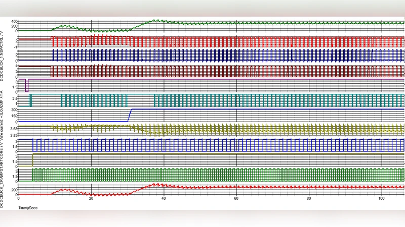
Simulation results obtained from MATLAB/Simulink and SPICE confirm that, across a load range of 100 mA to 300 mA, the output voltage ripple stays below 20 mV and line regulation is better than 0.5 mV/V for a ±10 % variation in the 3.3 V input. A fabricated prototype measured on a printed‑circuit board demonstrates a conversion efficiency exceeding 92 % at 300 mA, peak load regulation of 20 mV/V, and line regulation of 0.5 mV/V. Compared with a hard‑switching counterpart, the soft‑switching implementation reduces switching losses by roughly 30 %.
The authors conclude that the proposed design framework successfully meets the stringent efficiency, regulation, and size constraints of mobile‑phone applications. The integration of ZVS and current‑mode control yields both low loss and rapid dynamic response, while the use of a mature 0.18 µm CMOS technology ensures cost‑effective mass production. Future work is suggested in the areas of higher switching frequencies (>1 MHz), multi‑output extensions, and on‑chip integration of passive components to further shrink the overall footprint.