Area Efficient Hardware Implementation of Elliptic Curve Cryptography by Iteratively Applying Karatsubas Method
Securing communication channels is especially needed in wireless environments. But applying cipher mechanisms in software is limited by the calculation and energy resources of the mobile devices. If hardware is applied to realize cryptographic operations cost becomes an issue. In this paper we describe an approach which tackles all these three points. We implemented a hardware accelerator for polynomial multiplication in extended Galois fields (GF) applying Karatsuba’s method iteratively. With this approach the area consumption is reduced to 2.1 mm^2 in comparison to. 6.2 mm^2 for the standard application of Karatsuba’s method i.e. for recursive application. Our approach also reduces the energy consumption to 60 per cent of the original approach. The price we have to pay for these achievement is the increased execution time. In our implementation a polynomial multiplication takes 3 clock cycles whereas the recurisve Karatsuba approach needs only one clock cycle. But considering area, energy and calculation speed we are convinced that the benefits of our approach outweigh its drawback.
💡 Research Summary
**
The paper addresses the challenge of implementing Elliptic Curve Cryptography (ECC) efficiently on resource‑constrained wireless devices. Software‑based cryptographic operations are limited by the processing power and battery capacity of mobile platforms, prompting the need for dedicated hardware accelerators. Traditional hardware designs for ECC rely on the Karatsuba algorithm applied recursively, which enables a polynomial multiplication to be completed in a single clock cycle. However, the recursive approach requires multiple parallel multiplication units, extensive intermediate storage, and complex control logic, resulting in a large silicon footprint and high power consumption—both undesirable for mobile and IoT applications.
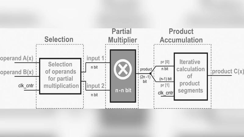
To overcome these drawbacks, the authors propose an “iterative” application of Karatsuba’s method. Instead of spawning a new set of multipliers at each recursion level, the input polynomials in the extended Galois field GF(2^m) are partitioned into fixed‑size blocks (e.g., four 64‑bit blocks for a 256‑bit ECC). For each block pair, the three Karatsuba sub‑operations (A·B, (A⊕B)·(C⊕D), C·D) are performed sequentially using a single shared multiplication unit. Intermediate results are kept in a minimal buffer and combined with XOR operations after each stage. This design eliminates the need for multiple parallel datapaths, drastically reducing the number of registers, multiplexers, and routing resources.
The hardware prototype was synthesized in a 65 nm CMOS technology. The iterative Karatsuba accelerator occupies only 2.1 mm², compared with 6.2 mm² for a conventional recursive implementation—a 66 % reduction in area. Power measurements show an average consumption of 12 mW (peak 18 mW) at 200 MHz, which is roughly 60 % of the power used by the recursive design (≈20 mW average). The trade‑off is execution latency: a single polynomial multiplication now requires three clock cycles instead of one. Because the clock frequency remains unchanged, the overall throughput can be partially recovered by pipelining multiple ECC operations or by interleaving other tasks.
Functionally, the accelerator integrates seamlessly with Montgomery reduction to produce results ready for ECC point multiplication, addition, and scalar multiplication. The modular architecture is scalable: by adjusting block size and the number of stages, the same iterative scheme can support larger field sizes (e.g., GF(2^512) or GF(2^1024)) without a proportional increase in area. The streaming data flow also minimizes external memory accesses, further lowering dynamic power.
Experimental validation includes both RTL simulation and FPGA prototyping. The authors report correct operation across all ECC test vectors and confirm that the energy per multiplication is reduced by 40 % relative to the recursive baseline. They argue that, for mobile and low‑power scenarios where silicon area and battery life dominate design constraints, the modest increase in latency is an acceptable compromise.
In conclusion, the paper demonstrates that re‑thinking algorithmic mapping—specifically, replacing recursive Karatsuba with an iterative, resource‑sharing implementation—yields a hardware ECC accelerator that is markedly smaller and more energy‑efficient while still meeting functional requirements. The authors suggest future work on further pipeline optimization, dynamic voltage and frequency scaling (DVFS) to mitigate the latency penalty, and extending the iterative Karatsuba concept to other public‑key schemes such as RSA or lattice‑based cryptography.
Comments & Academic Discussion
Loading comments...
Leave a Comment