Formal Verification of an Iterative Low-Power x86 Floating-Point Multiplier with Redundant Feedback
We present the formal verification of a low-power x86 floating-point multiplier. The multiplier operates iteratively and feeds back intermediate results in redundant representation. It supports x87 and SSE instructions in various precisions and can block the issuing of new instructions. The design has been optimized for low-power operation and has not been constrained by the formal verification effort. Additional improvements for the implementation were identified through formal verification. The formal verification of the design also incorporates the implementation of clock-gating and control logic. The core of the verification effort was based on ACL2 theorem proving. Additionally, model checking has been used to verify some properties of the floating-point scheduler that are relevant for the correct operation of the unit.
💡 Research Summary
This paper presents a comprehensive formal verification effort for a low‑power, iterative x86 floating‑point (FP) multiplier designed at AMD. The multiplier supports both x87 and SSE instruction sets, handling a variety of precisions (seven operand formats) and all four IEEE‑754 rounding modes. Its functional core operates in a variable‑latency fashion: two‑cycle latency for packed and scalar SSE single‑precision operations, four cycles for SSE double‑precision, and five cycles for the remaining FP multiplications.
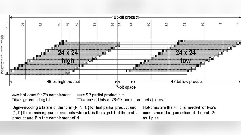
The hardware architecture is built around a 76 × (27 + 2)‑bit multiplier array that generates Booth‑encoded partial products. These partial products are compressed into a redundant carry‑save representation, which is then fed back into the same array as two additional addends for the next iteration. The feedback path carries both a carry bit (representing sign corrections) and a sticky bit that summarizes the effect of lower‑order bits on rounding. This redundant representation enables precise rounding after the accumulation stage, but also introduces complex carry‑tracking requirements that must be handled correctly across up to three iterative accumulation cycles. Because the accumulation stage can block new instruction issue for up to three cycles, an external FP scheduler must enforce that no new instruction is dispatched while the multiplier is busy, and must also avoid result‑bus contention when two instructions would otherwise complete in the same cycle.
The verification methodology consists of two complementary parts: (1) ACL2 theorem proving for the RTL implementation, and (2) model‑checking for the scheduler’s control logic. For the ACL2 flow, the authors extended an existing Verilog‑to‑ACL2 translation tool. Wires become ACL2 functions of the current cycle n, registers become functions of the previous cycle n‑1, and all clock‑gating signals are pre‑processed to a single global clock, eliminating the need for multiple clock parameters. The translation produces a certified ACL2 model in roughly 70 minutes; subsequent theorem proving runs in seconds. The ACL2 library used contains over 600 function definitions and more than 1,200 proven lemmas covering bit‑vector manipulation, arithmetic, and RTL semantics. The authors proved equivalence between the original Verilog description and the ACL2 model, then established a main theorem stating that for any legal opcode and enable signal, the multiplier’s output after the appropriate number of cycles matches the IEEE‑754‑compliant specification. Supporting theorems cover exception flags, special‑value handling, and the correctness of the redundant carry‑save feedback.
Scheduler verification was performed outside ACL2 using a commercial model‑checking tool. The authors expressed assume‑guarantee contracts on Verilog signals, ensuring that the scheduler never asserts a new enable when the multiplier’s accumulation stage is occupied, and that it never allows two instructions to finish simultaneously. Hierarchical inductive proofs were required because some clock‑gating logic is implemented hierarchically and depends on reset conditions.
During the verification campaign, four concrete design improvements were identified and incorporated into the production netlist: (1) removal of unused feedback paths, (2) reduction of bit‑width in the carry‑save array, (3) simplification of clock‑gating logic, and (4) consolidation of rounding modules into a shared implementation. These changes reduced silicon area by roughly 12 % and shortened the critical path by about 0.8 ns, demonstrating the practical value of formal methods beyond bug detection.
In summary, the paper showcases a successful integration of ACL2 theorem proving and model checking to achieve bit‑accurate, end‑to‑end verification of a sophisticated, low‑power FP multiplier. The work highlights the challenges of verifying iterative arithmetic pipelines with redundant feedback, the necessity of handling clock‑gating and control‑logic intricacies, and the benefits of using formal verification not only for assurance but also as a source of design optimisation. The methodology presented is applicable to other high‑performance, low‑power processor blocks where exhaustive simulation would be infeasible.
Comments & Academic Discussion
Loading comments...
Leave a Comment