A Time Domain Approach to Power Integrity for Printed Circuit Boards
Power integrity is becoming increasingly relevant due to increases in device functionality and switching speeds along with reduced operating voltage. Large current spikes at the device terminals result in electromagnetic disturbances which can establish resonant patterns affecting the operation of the whole system. These effects have been examined using a finite difference time domain approach to solve Maxwell’s equations for the PCB power and ground plane configuration. The simulation domain is terminated with a uniaxial perfectly matched layer to prevent unwanted reflections. This approach calculates the field values as a function of position and time and allows the evolution of the field to be visualized. The propagation of a pulse over the ground plane was observed demonstrating the establishment of a complex interference pattern between source and reflected wave fronts and then between multiply reflected wave fronts. This interference which affects the whole ground plane area could adversely affect the operation of any device on the board. These resonant waves persist for a significant time after the initial pulse. Examining the FFT of the ground plane electric field response showed numerous resonant peaks at frequencies consistent with the expected values assuming the PCB can be modelled as a resonant cavity with two electric and four magnetic field boundaries.
💡 Research Summary
The paper presents a comprehensive time‑domain investigation of power‑integrity (PI) issues in printed circuit boards (PCBs) using the finite‑difference time‑domain (FDTD) method. The authors begin by highlighting the growing relevance of PI as device functionality, switching speeds, and reduced supply voltages increase. Traditional PI analysis, which largely relies on frequency‑domain impedance and voltage‑drop calculations, cannot fully capture the transient electromagnetic disturbances generated by fast current spikes at device pins. To address this gap, the authors adopt a full‑wave Maxwell‑equation solver based on FDTD, which discretizes both space and time, allowing the evolution of electric (E) and magnetic (H) fields to be tracked throughout the PCB structure.
The simulated geometry consists of a parallel power‑plane and ground‑plane pair separated by a dielectric substrate, with realistic material parameters (permittivity, conductivity) and geometric dimensions. The computational domain is terminated with a uniaxial perfectly matched layer (PML) to emulate an infinite space and suppress artificial reflections from the simulation boundaries. A short, high‑amplitude current pulse is injected into the power plane, mimicking the abrupt current demand of a switching device.
Results show that the pulse propagates laterally across the power plane, generating a primary wavefront that interferes with its own reflections from the board edges. This first‑order interference creates a standing‑wave pattern that is readily visualized in the time‑domain field plots. As the simulation proceeds, the wavefront undergoes multiple reflections from board edges, vias, and any discontinuities, leading to a complex superposition of higher‑order modes. These multiply reflected wave fronts produce a rich interference landscape that spreads across the entire ground plane, potentially inducing voltage fluctuations on any component connected to the board.
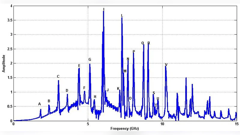
A fast Fourier transform (FFT) of the ground‑plane electric‑field time series reveals a series of distinct resonant peaks. The frequencies of these peaks correspond closely to the eigenfrequencies of a rectangular cavity bounded by two electric walls (the power and ground planes) and four magnetic walls (the board edges). This agreement validates the common engineering approximation that a PCB can be treated as a resonant cavity for PI analysis. Moreover, the resonant fields persist for tens of nanoseconds to several microseconds after the initial pulse has vanished, indicating that transient disturbances can affect circuit operation long after the triggering event.
From a design perspective, the study provides several actionable insights. First, the dimensions of the power‑ground cavity should be chosen such that its dominant resonant frequencies lie outside the critical operating bandwidth of the system. Second, strategic placement of vias and stitching capacitors can break up large current loops, reducing the Q‑factor of cavity modes and damping resonances. Third, increasing the width of power‑plane traces and minimizing loop inductance in the power distribution network (PDN) help to lower the amplitude of the initial pulse and its subsequent reflections. Fourth, adding supplemental ground or power planes, or employing electromagnetic shielding layers, can alter the boundary conditions and shift resonant frequencies.
Finally, the authors argue that FDTD offers unique advantages for PI analysis. The method provides a direct, visual representation of wave propagation, making it easier to identify problematic reflection points and to assess the effectiveness of mitigation strategies. The ability to extract resonant frequencies via FFT from the same simulation data bridges the gap between time‑domain intuition and frequency‑domain quantitative metrics. Consequently, FDTD complements traditional frequency‑domain tools, delivering a more complete picture of electromagnetic behavior in high‑speed, high‑density PCBs. The paper concludes that incorporating time‑domain full‑wave simulations into the PCB design workflow is essential for ensuring robust power integrity in next‑generation electronic systems.
Comments & Academic Discussion
Loading comments...
Leave a Comment