Band Gap Optimization of Two-Dimensional Photonic Crystals Using Semidefinite Programming and Subspace Methods
In this paper, we consider the optimal design of photonic crystal band structures for two-dimensional square lattices. The mathematical formulation of the band gap optimization problem leads to an infinite-dimensional Hermitian eigenvalue optimization problem parametrized by the dielectric material and the wave vector. To make the problem tractable, the original eigenvalue problem is discretized using the finite element method into a series of finite-dimensional eigenvalue problems for multiple values of the wave vector parameter. The resulting optimization problem is large-scale and non-convex, with low regularity and non-differentiable objective. By restricting to appropriate eigenspaces, we reduce the large-scale non-convex optimization problem via reparametrization to a sequence of small-scale convex semidefinite programs (SDPs) for which modern SDP solvers can be efficiently applied. Numerical results are presented for both transverse magnetic (TM) and transverse electric (TE) polarizations at several frequency bands. The optimized structures exhibit patterns which go far beyond typical physical intuition on periodic media design.
💡 Research Summary
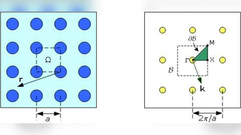
The paper addresses the challenging problem of maximizing photonic‑crystal band‑gaps for two‑dimensional square‑lattice structures. Physically, the band‑gap is the difference between the smallest eigenvalue of the (n + 1)‑th Bloch mode and the largest eigenvalue of the n‑th mode, both of which depend on the spatially varying dielectric function ε(r) and the Bloch wave‑vector k. This “max‑min” objective is non‑convex, non‑smooth, and involves an infinite‑dimensional Hermitian eigenvalue problem.
To obtain a tractable formulation, the authors discretize the governing Maxwell equations with the finite‑element method (FEM). The unit cell is meshed, and ε is represented as a piecewise‑constant material parameter that can take either a low‑index value ε_low or a high‑index value ε_high (or a convex combination thereof). For each sampled k‑point in the irreducible Brillouin zone, a finite‑dimensional Hermitian matrix A(ε,k) is assembled, and its eigenvalues λ₁≤λ₂≤… are computed. The overall optimization therefore consists of many eigenvalue problems (one per k‑point) coupled through the common design variable ε.
Directly optimizing the band‑gap is infeasible because the objective is non‑differentiable and the feasible set is highly non‑convex. The key insight of the work is to restrict attention to the eigenspaces that actually define the gap edges. Let Uₗ be the subspace spanned by the eigenvectors associated with the n‑th band (the lower edge) and Uᵤ the subspace spanned by the eigenvectors of the (n + 1)‑th band (the upper edge). For any vector x∈Uₗ we have xᵀA(ε,k)x ≤ γₗ, and for any y∈Uᵤ we have yᵀA(ε,k)y ≥ γᵤ, where γₗ and γᵤ are scalar variables representing the lower and upper gap bounds. These inequalities are linear matrix inequalities (LMIs) in the design variables because A depends linearly on ε. Consequently, the original non‑convex problem can be reformulated as a convex semidefinite program (SDP): maximize γᵤ − γₗ subject to the LMIs for all sampled k‑points and to material‑parameter bounds ε_low ≤ ε(r) ≤ ε_high.
The algorithm proceeds iteratively. Starting from an initial ε (e.g., a uniform background), the FEM eigenvalue problems are solved, the relevant eigenvectors are extracted, and the subspaces Uₗ, Uᵤ are built. With these subspaces fixed, an SDP is solved to obtain an updated ε and new gap bounds. The updated ε is then used to recompute the eigenvectors, and the process repeats until the change in the gap or in ε falls below a prescribed tolerance. Because each SDP is relatively small (its size is determined by the dimension of the chosen subspaces, not by the full FEM mesh), modern interior‑point SDP solvers can handle it efficiently. In practice, 10–20 iterations are sufficient for convergence.
Numerical experiments are presented for both transverse‑magnetic (TM) and transverse‑electric (TE) polarizations and for several frequency bands (e.g., TM 1‑2, TE 3‑4). The optimized designs exhibit highly non‑intuitive patterns: instead of simple circular or square holes, the algorithm produces intricate, asymmetric “ribbon‑like” or multi‑hole motifs that significantly enlarge the band‑gap (up to ~30 % improvement over conventional designs). The results demonstrate that the subspace‑SDP framework can explore design regions that are inaccessible to intuition‑driven approaches.
Beyond the specific 2‑D case, the authors discuss extensions to three‑dimensional photonic crystals, non‑regular lattices, and even nonlinear material models, because the core idea—projecting the infinite‑dimensional eigenvalue problem onto the active eigenspaces and then enforcing eigenvalue bounds via LMIs—remains valid. The combination of FEM for accurate physics, subspace reduction for dimensionality control, and SDP for convex optimization yields a powerful, scalable methodology for photonic‑crystal band‑gap engineering.
Comments & Academic Discussion
Loading comments...
Leave a Comment