Subwavelength Nanopatch Cavities for Semiconductor Plasmon Lasers
We propose and analyze a family of nanoscale cavities for electrically-pumped surface-emitting semiconductor lasers that use surface plasmons to provide optical mode confinement in cavities which have dimensions in the 100-300 nm range. The proposed laser cavities are in many ways nanoscale optical versions of micropatch antennas that are commonly used at microwave/RF frequencies. Surface plasmons are not only used for mode confinement but also for output beam shaping to realize single-lobe far-field radiation patterns with narrow beam waists from subwavelength size cavities. We identify the cavity modes with the largest quality factors and modal gain, and show that in the near-IR wavelength range (1.0-1.6 microns) cavity losses (including surface plasmon losses) can be compensated by the strong mode confinement in the gain region provided by the surface plasmons themselves and the required material threshold gain values can be smaller than 700 1/cm.
💡 Research Summary
The paper introduces a novel class of electrically pumped, surface‑emitting semiconductor lasers built around sub‑wavelength “nanopatch” cavities whose lateral dimensions range from 100 nm to 300 nm. The architecture consists of a bulk III‑V gain medium (typically InGaAsP) sandwiched between two thick silver layers, forming a metal‑insulator‑metal (MIM) waveguide that simultaneously confines the optical mode via surface plasmon polaritons (SPPs) and serves as the electrical contacts for current injection. The metal layers act as antenna reflectors, directing the radiation upward and giving the device its surface‑emitting character.
The authors focus on circular nanopatch cavities for computational convenience, but also discuss rectangular and hexagonal variants, noting that the modal characteristics are qualitatively similar. Because the cavity is much smaller than the free‑space wavelength, conventional dielectric feedback (e.g., Bragg mirrors) would require many periods and thus a larger overall footprint. By exploiting the high wave‑vector of SPPs away from the metal plasma resonance, the authors achieve strong confinement while keeping propagation loss at a manageable level in the near‑infrared (1.0–1.6 µm).
Through full‑vector 3‑D eigenmode solving and finite‑difference‑time‑domain (FDTD) simulations, the paper identifies the TM₁₁₁ mode as the most favorable. This mode exhibits a vertical electric field component (E_z) that is symmetric about the cavity mid‑plane, while the transverse components (E_r, E_φ) are antisymmetric. Such symmetry leads to partial cancellation of far‑field radiation from the top and bottom of the cavity, reducing radiative loss (Q_r) and enhancing the overall quality factor (Q ≈ 30–150). Moreover, the field distribution overlaps strongly with the gain region, yielding an energy confinement factor Γ_e of 0.6–0.8.
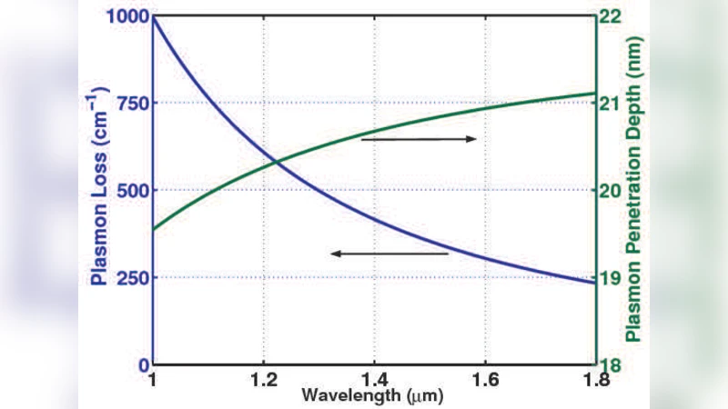
Material parameters are taken from experimentally measured silver permittivity (Johnson‑Christy data) and fitted with a Drude‑type plasma dispersion model (ε(ω)=ε_∞−ω_p²/
Comments & Academic Discussion
Loading comments...
Leave a Comment