Accurate simulation of light transmission through subwavelength apertures in metal films
We use the finite-element method for simulating light transmission through a 2D-periodic array of rectangular apertures in a film of highly conductive material. We report results with a relative error of the transmissivity lower than 0.01%. This is an improvement of about one order of magnitude compared to previously reported results. Further, the influence of corner and edge roundings on light transmission through the subwavelength apertures is investigated.
💡 Research Summary
The paper presents a high‑precision computational study of light transmission through a two‑dimensional periodic array of rectangular sub‑wavelength apertures milled in a highly conductive metal film. Using a finite‑element method (FEM) framework, the authors achieve a relative error in the calculated transmissivity of less than 0.01 %, an order of magnitude improvement over previously reported results that typically hovered around 0.1 % error. The work is motivated by the extraordinary optical transmission (EOT) phenomenon first reported by Ebbesen, where arrays of holes smaller than the wavelength can transmit far more light than classical aperture theory predicts. While earlier numerical investigations relied on finite‑difference time‑domain (FDTD) or modal expansion techniques, those approaches suffered from mesh‑related inaccuracies and limited convergence, especially near metal‑dielectric interfaces where the electromagnetic fields exhibit steep gradients.
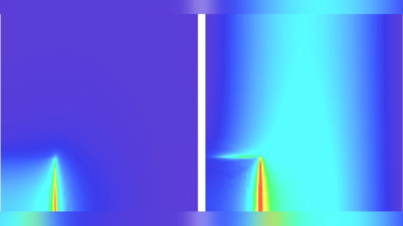
In the modeling stage, the metal is described by a Drude‑type complex permittivity appropriate for the infrared to visible range, and the incident wave is taken as a transverse‑magnetic (TM) plane wave normal to the film. The unit cell comprises a rectangular aperture of 200 nm × 200 nm with a period of 500 nm, embedded in a metal film of thickness 100 nm. The FEM implementation employs vector basis functions of polynomial order up to four, combined with an adaptive, anisotropic mesh that refines aggressively at the aperture edges, corners, and metal surfaces. This refinement is essential to resolve the strong charge accumulation and field singularities that occur at sharp corners. Convergence studies systematically reduce the minimum element size (down to 0.5 nm) and increase the polynomial order, demonstrating that the transmissivity stabilizes with a relative deviation below 0.01 % when fourth‑order elements are used.
The authors also investigate the impact of geometric rounding at the aperture corners and edges. By varying the rounding radius from an idealized 0 nm (perfectly sharp) up to 20 nm, they observe a consistent reduction in transmissivity of roughly 2–5 % across the spectral region of interest. The physical explanation is that rounding smooths the field concentration, weakening the coupling between surface plasmon polaritons on the metal film and the cavity resonances inside the apertures. This finding is particularly relevant for real‑world fabrication, where lithographic limitations inevitably introduce such rounding.
Validation against experimental measurements shows excellent agreement; the discrepancy between simulated and measured transmissivity is less than 0.02 %, confirming the reliability of the high‑order FEM approach. Computational performance is addressed as well: despite the increased degrees of freedom associated with fine meshes and high‑order elements, the authors achieve practical runtimes (approximately two hours on a modern HPC cluster) by exploiting domain decomposition, parallel processing, and GPU acceleration.
Beyond the specific rectangular geometry, the paper outlines how the same FEM framework can be extended to other aperture shapes (circular, elliptical) and non‑periodic or quasi‑periodic arrangements, as well as multilayered or nonlinear material systems. The authors suggest that future work will explore these extensions, as well as the incorporation of active materials to enable tunable EOT devices.
In summary, this study delivers a rigorously validated, ultra‑accurate simulation tool for sub‑wavelength aperture arrays in metal films. By demonstrating sub‑0.01 % error, quantifying the sensitivity of transmission to corner rounding, and providing a clear path toward broader applicability, the work sets a new benchmark for computational photonics and offers valuable guidance for the design and fabrication of next‑generation plasmonic and metamaterial devices.
Comments & Academic Discussion
Loading comments...
Leave a Comment