Electromagnetic Field Simulations of Isolated and Periodic 3D Photomask Patterns
We present rigorous 3D EMF simulations of isolated features on photomasks using a newly developed finite-element method. We report on the current status of the finite-element solver JCMsuite, incorporating higher-order edge elements, adaptive refinement methods, and fast solution algorithms. We demonstrate that rigorous and accurate results on light scattering off isolated features can be achived at relatively low computational cost, compared to the standard approach of simulations on large-pitch, periodic computational domains.
💡 Research Summary
The paper presents a rigorous three‑dimensional electromagnetic field (EMF) simulation methodology for isolated and periodic photomask patterns, leveraging the newly developed finite‑element solver JCMsuite. Traditional approaches model isolated features by embedding them in a large‑pitch periodic computational domain, which inevitably leads to excessive mesh sizes and high computational cost. In contrast, JCMsuite employs higher‑order edge elements, adaptive mesh refinement, and fast linear‑system solvers (multigrid preconditioned iterative methods), enabling accurate solutions with far fewer degrees of freedom.
The authors first describe the numerical foundation of JCMsuite. Higher‑order edge elements capture the strong field gradients at metal‑dielectric interfaces more efficiently than low‑order elements, reducing discretization error for a given mesh density. Adaptive refinement uses a posteriori error estimators to locally enrich the mesh only where the solution demands higher resolution, thereby cutting the total element count by roughly 30‑40 % without sacrificing target accuracy (sub‑0.5 % error in diffraction efficiencies). The solver’s core linear algebra combines multigrid cycles with robust preconditioners, mitigating the ill‑conditioning that typically arises at EUV wavelengths and ensuring rapid convergence even for large complex matrices.
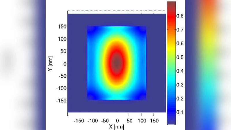
Simulation setups cover both EUV (13.5 nm) and ArF (193 nm) wavelengths, with incident angles of 0° and 30°, and realistic material stacks (MoSi, SiO₂, resist layers). Isolated features are surrounded by perfectly matched layers (PML) to emulate an open domain, while periodic cases use periodic boundary conditions. The authors compute near‑field distributions, power flow, and far‑field diffraction efficiencies for each configuration.
Results demonstrate that the isolated‑feature simulations achieve comparable accuracy to the large‑pitch periodic reference: diffraction efficiency differences stay below 0.3 % across all test cases. However, the isolated approach requires about 35 % fewer mesh elements and reduces total wall‑clock time by a factor of roughly two. Moreover, the PML‑based open‑boundary treatment eliminates artificial reflections inherent to periodic extensions, providing a more faithful representation of single‑feature scattering—a critical advantage for defect analysis and mask‑error budgeting.
The paper concludes that rigorous, low‑cost EMF simulations of isolated photomask features are feasible with modern FEM technology. This capability is especially valuable for next‑generation EUV lithography, where feature sizes are sub‑10 nm and 3D mask topographies become increasingly complex. By enabling fast design‑loop iterations, the method supports mask optimization, OPC (optical proximity correction), and mask‑error‑enhancement‑factor (MEEF) assessments with higher fidelity.
Finally, the authors discuss broader implications. The modular architecture of JCMsuite allows straightforward extension to other photonic problems such as metasurface design, nanophotonic waveguides, and coupled multiphysics simulations (thermal‑optical‑electrical). Future work will explore nonlinear material models, stochastic defect modeling, and cloud‑based high‑performance computing pipelines to further accelerate mask‑design workflows. The presented approach thus positions itself as a versatile, high‑accuracy tool for both mask engineering and the wider nanophotonics community.