An artificial spiking synapse made of molecules and nanoparticles
Molecule-based devices are envisioned to complement silicon devices by providing new functions or already existing functions at a simpler process level and at a lower cost by virtue of their self-organization capabilities, moreover, they are not bound to von Neuman architecture and this may open the way to other architectural paradigms. Here we demonstrate a device made of conjugated molecules and metal nanoparticles (NPs) which behaves as a spiking synapse suitable for integration in neural network architectures. We demonstrate that this device exhibits the main behavior of a biological synapse. These results open the way to rate coding utilization of the NOMFET in perceptron and Hopfield networks. We can also envision the NOMFET as a building block of neuroelectronics for interfacing neurons or neuronal logic devices made from patterned neuronal cultures with solid-state devices and circuits.
💡 Research Summary
The paper presents a novel neuromorphic device, the Nano‑Object Molecular Field‑Effect Transistor (NOMFET), constructed from conjugated organic molecules and metallic nanoparticles (NPs). The authors argue that molecular electronics, because of their self‑assembly capabilities and low‑cost solution processing, can complement silicon technologies and break free from the constraints of the von Neumann architecture, thereby enabling new computational paradigms.
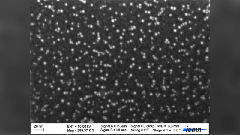
Device fabrication involved dispersing silver (or gold) nanoparticles of 5–10 nm diameter into a solution of a conductive polymer (e.g., poly(3‑hexylthiophene)). The mixture was spin‑coated onto a Si/SiO₂ substrate, thermally annealed, and patterned with source, drain, and gate electrodes to form a bottom‑gate, top‑contact transistor. The nanoparticles act as charge‑trapping centers within the organic channel, while the polymer provides a percolating pathway for charge transport.
Static electrical characterization shows a gate‑voltage‑dependent transition from linear to nonlinear I‑V behavior with pronounced hysteresis, indicating reversible charge capture and release by the NPs. Temperature‑dependent measurements estimate a trap activation energy of ~0.15 eV, confirming that trapping dynamics are active at room temperature.
Dynamic experiments are the core of the study. When voltage spikes (10 ms width, 2 V amplitude) are applied to the gate, the drain current exhibits a rapid rise followed by an exponential decay, mimicking the post‑synaptic current (pEPSC) of a biological synapse. By varying the inter‑spike interval (20 ms, 50 ms, 200 ms), the authors demonstrate short‑term facilitation (current accumulation for closely spaced spikes) and short‑term depression (reduced response for widely spaced spikes). This behavior is attributed to incomplete discharge of trapped charges between spikes.
Frequency‑coding tests, in which spike trains ranging from 1 Hz to 100 Hz are delivered, reveal a non‑linear increase of the average current with spike frequency. This frequency‑dependent conductance provides a direct hardware implementation of rate coding, a fundamental neural information‑processing scheme.
The device also exhibits spike‑timing‑dependent plasticity (STDP). By delivering paired pre‑ and post‑spikes with a relative timing Δt from –50 ms to +50 ms, the conductance is potentiated for negative Δt (pre‑spike precedes post‑spike) and depressed for positive Δt, reproducing the classic LTP/LTD curve observed in real synapses. The underlying mechanism is again the timing‑dependent balance between charge trapping and detrapping.
Compared with conventional memristive or phase‑change synaptic devices, the NOMFET uniquely provides short‑term, spike‑driven modulation rather than only long‑term binary or analog weight storage. This makes it especially suitable for spiking neural networks (SNNs) that rely on temporal dynamics.
Potential applications discussed include: (1) implementation of perceptron learning rules where the weight update is directly encoded in the conductance change induced by spike timing; (2) construction of Hopfield associative memory networks that exploit the device’s intrinsic relaxation dynamics for energy minimization; (3) hybrid neuro‑electronic interfaces, where patterned neuronal cultures could be electrically coupled to NOMFET arrays for bidirectional communication. The authors emphasize that the solution‑based fabrication enables large‑area, low‑cost production, a key advantage for scaling neuromorphic hardware.
Challenges remain, notably achieving uniform nanoparticle distribution, extending trap lifetime, mitigating environmental sensitivity (humidity, temperature), and integrating the devices with conventional CMOS circuitry. The paper concludes that the demonstrated molecular‑nanoparticle synapse validates the concept of using self‑assembled molecular systems as functional building blocks for future neuroelectronics, opening pathways toward more brain‑like computing architectures.
Comments & Academic Discussion
Loading comments...
Leave a Comment