A novel way of filling high aspect ratio vertical interconnection (microvias) with an aspect ratio of >2:1 is presented. High frequency acoustic streaming at megasonic frequencies enables the decrease of the Nernst-diffusion layer down to the sub-micron range, allowing thereby conformal electrodeposition in deep grooves. Higher throughput and better control over the deposition properties are possible for the manufacturing of interconnections and metal-based MEMS.
Deep Dive into Megasonic Enhanced Electrodeposition.
A novel way of filling high aspect ratio vertical interconnection (microvias) with an aspect ratio of >2:1 is presented. High frequency acoustic streaming at megasonic frequencies enables the decrease of the Nernst-diffusion layer down to the sub-micron range, allowing thereby conformal electrodeposition in deep grooves. Higher throughput and better control over the deposition properties are possible for the manufacturing of interconnections and metal-based MEMS.
9-11 April 2008
© EDA Publishing/DTIP 2008
ISBN: 978-2-35500-006-5
Megasonic Enhanced Electrodeposition
Jens Kaufmann1, Marc P.Y. Desmulliez1, Dennis Price2
[1] MicroSystems Engineering Centre (MISEC), School of Engineering & Physical Science,
Heriot Watt University, Edinburgh, EH14 4AS, United Kingdom
[2] Merlin Circuit Technology LTD,Harwarden Industrial ParkManor Lane,
Deeside, Flintshire,West Wales, CH5 3QZ, United Kingdom
Abstract A novel way of filling high aspect ratio vertical
interconnection (microvias) is presented. High frequency
acoustic streaming at megasonic frequencies enables the
decrease of the Nernst-diffusion layer down to the sub-micron
range, allowing thereby conformal electrodeposition in deep
grooves. Higher throughput and better control over the
deposition
properties
are
therefore
possible
for
the
manufacturing of interconnections and metal-based MEMS.
I.
INTRODUCTION
The increasing consumer demand for faster, lighter and
smarter electronic devices calls for enhanced system
integration and packaging technologies. Key to the
increasing density of electronic components is the
introduction of the high density interconnection (HDI)
technology in printed circuit boards (PCB), resulting in
multilayer technology and increasing amounts of electrical
connections that need to be handled. Microvias are elements
that are particularly important as they allow the reduction of
the footprint of electronic components through the
redistribution of interconnects in the underlying layers.
Microvias are formed by mechanical drilling or laser
ablation of the PCB material and subsequent electroplating is
used to fill the cavity to render them electrically conductive.
The microvias need however a conductive seed layer on the
side walls to allow the electrodeposition of metal. The
technologies used in that respect are mainly autocatalytic
plating processes or direct metallisation[1].
To allow further integration and miniaturization, it is
necessary to form microvias with an aspect ratio (height over
diameter hole ratio) greater than 1:1. This current limit arises
because of the difficult hydrodynamic conditions and current
crowding effect at the mouth of the hole; both conditions
attenuate the convection in the electrolytic solution near the
surface of the substrate. This lack of effective agitation
reduces the ion concentration in the solution within the
immediate proximity of the microvia, increases the Nernst
diffusion layer and limits therefore the deposition rate of the
metal [2]. To overcome this limitation, extensive research
utilising a variety of additives and current waveforms was
performed. The additives used are mainly large organic
inhibitors, and small complex builders that accelerate the
deposition at the bottom of the via cavity. This is a very
complex method, which needs a carefully controlled
solution. However, super conformal plating of deep trenches
and holes can be achieved, as exampled by the damascene
process metallisation. The use of this process in high volume
consumer electronics would nevertheless be problematic
because of the high parameter variants found in the usually
large volumes of solution used in PCM manufacturing. This
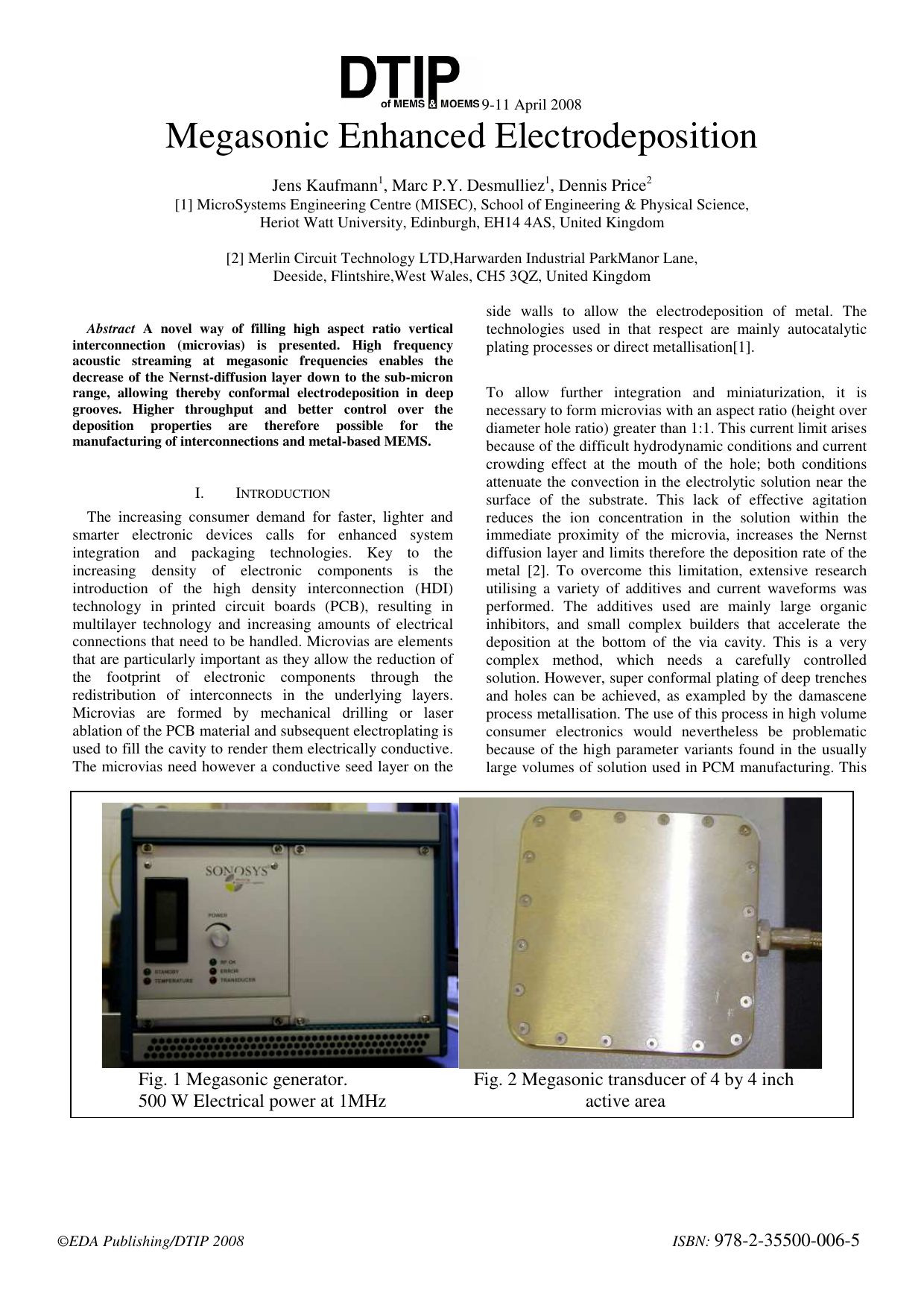
Fig. 1 Megasonic generator.
Fig. 2 Megasonic transducer of 4 by 4 inch
500 W Electrical power at 1MHz
active area
9-11 April 2008
© EDA Publishing/DTIP 2008
ISBN: 978-2-35500-006-5
paper proposes therefore to use megasonic agitation to
reduce
the
diffusion
layer
and
achieve
optimal
electrodeposition for microvias with aspect ratio larger than
1:1.
II.
MEGASONIC AGITATION
This paper describes a new method to enhance the
capability and compatibility of metallisation processes based
on megasonic assisted copper electrodeposition. The primary
focus of this article concerns the filling of high aspect ratio
microvias. However, this technology is transferable to the
manufacture of various high aspect ratio metal MEMS
structures as well as the development of photoresist in deep
trenches. A high frequency acoustic streaming of frequency f
allows the modification of the near surface hydrodynamics.
The electrical potential of the ox-red reaction is governed by
the activity of the ion near the electrode surface, according to
the Nernst equation:
d
OZ
e
a
a
F
z
RT
E
E
Re
0
ln
+
(1)
Increasing the activity, a, and therefore the concentration,
c, near the surface of the substrate, results in a decreased
overpotential.
(
)
+
⋅
=
Z
M
M
c
a
Z
γ
(2)
δ
0c
dx
dc =
(3)
More precisely, the Nernst diffusion layer which, in
normal conditions, is governed by the velocity of the
medium stream over the solid surface, as in (4), see [3],
depends on 1/f1/2 in the presence of an acoustic field, as in
(5).
2
1
16
.
0
Ux
v
ic
Hydrodynam
δ
(4)
2
1
2
ω
δ
v
acoustic
(5)
The h
…(Full text truncated)…
This content is AI-processed based on ArXiv data.