Microcantilever specimens for in-plane and out-ofplane bending tests are here analyzed. Experimental validation of 2D and 3D numerical models is performed. Main features of in-plane and out-of-plane layouts are then discussed. Effectiveness of plane models to predict pull-in in presence of geometric nonlinearity due to a large tip displacement and initial curvature of microbeam is investigated. The paper is aimed to discuss the capability of 2D models to be used as compact tools to substitute some model order reduction techniques, which appear unsuitable in presence of both electromechanical and geometric nonlinearities.
Deep Dive into Validation of compact models of microcantilever actuators for RF-MEMS application.
Microcantilever specimens for in-plane and out-ofplane bending tests are here analyzed. Experimental validation of 2D and 3D numerical models is performed. Main features of in-plane and out-of-plane layouts are then discussed. Effectiveness of plane models to predict pull-in in presence of geometric nonlinearity due to a large tip displacement and initial curvature of microbeam is investigated. The paper is aimed to discuss the capability of 2D models to be used as compact tools to substitute some model order reduction techniques, which appear unsuitable in presence of both electromechanical and geometric nonlinearities.
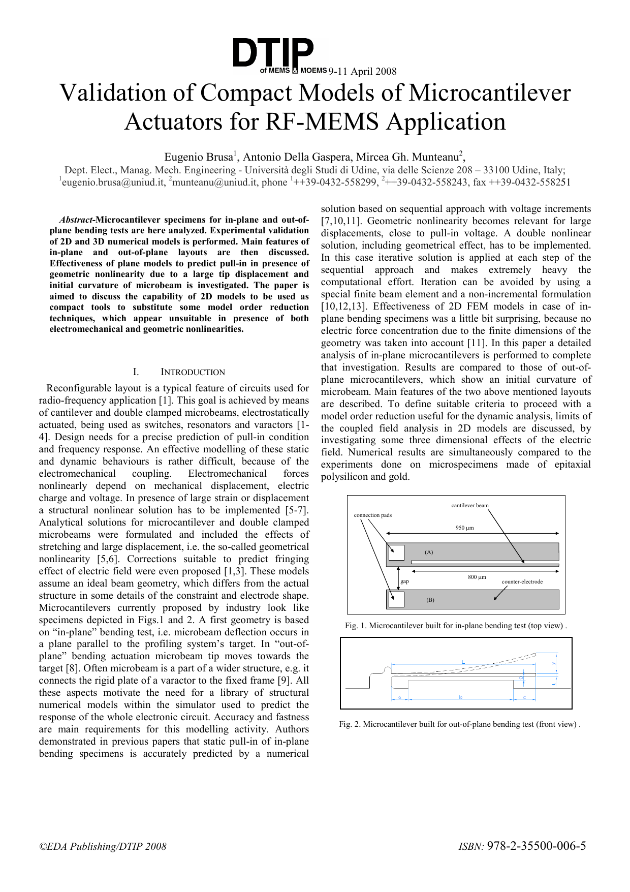
Reconfigurable layout is a typical feature of circuits used for radio-frequency application [1]. This goal is achieved by means of cantilever and double clamped microbeams, electrostatically actuated, being used as switches, resonators and varactors [1][2][3][4]. Design needs for a precise prediction of pull-in condition and frequency response. An effective modelling of these static and dynamic behaviours is rather difficult, because of the electromechanical coupling. Electromechanical forces nonlinearly depend on mechanical displacement, electric charge and voltage. In presence of large strain or displacement a structural nonlinear solution has to be implemented [5][6][7]. Analytical solutions for microcantilever and double clamped microbeams were formulated and included the effects of stretching and large displacement, i.e. the so-called geometrical nonlinearity [5,6]. Corrections suitable to predict fringing effect of electric field were even proposed [1,3]. These models assume an ideal beam geometry, which differs from the actual structure in some details of the constraint and electrode shape. Microcantilevers currently proposed by industry look like specimens depicted in Figs. 1 and2. A first geometry is based on "in-plane" bending test, i.e. microbeam deflection occurs in a plane parallel to the profiling system's target. In "out-ofplane" bending actuation microbeam tip moves towards the target [8]. Often microbeam is a part of a wider structure, e.g. it connects the rigid plate of a varactor to the fixed frame [9]. All these aspects motivate the need for a library of structural numerical models within the simulator used to predict the response of the whole electronic circuit. Accuracy and fastness are main requirements for this modelling activity. Authors demonstrated in previous papers that static pull-in of in-plane bending specimens is accurately predicted by a numerical solution based on sequential approach with voltage increments [7,10,11]. Geometric nonlinearity becomes relevant for large displacements, close to pull-in voltage. A double nonlinear solution, including geometrical effect, has to be implemented. In this case iterative solution is applied at each step of the sequential approach and makes extremely heavy the computational effort. Iteration can be avoided by using a special finite beam element and a non-incremental formulation [10,12,13]. Effectiveness of 2D FEM models in case of inplane bending specimens was a little bit surprising, because no electric force concentration due to the finite dimensions of the geometry was taken into account [11]. In this paper a detailed analysis of in-plane microcantilevers is performed to complete that investigation. Results are compared to those of out-ofplane microcantilevers, which show an initial curvature of microbeam. Main features of the two above mentioned layouts are described. To define suitable criteria to proceed with a model order reduction useful for the dynamic analysis, limits of the coupled field analysis in 2D models are discussed, by investigating some three dimensional effects of the electric field. Numerical results are simultaneously compared to the experiments done on microspecimens made of epitaxial polysilicon and gold. Experimental validation of numerical models developed in previous papers was performed on eight geometries, described in Table I. FEM static analysis was performed in ANSYS code, as sequential solution with mesh morphing in dielectric region, then through the non-incremental FEM sequential approach tested in [10,12,13] and by a combined sequential FEM/BEM solution [11]. Last two methods were implemented in Matlab. An additional comparison included results of the Discrete Geometric Approach (DGA), recently proposed [14]. As Fig. 3 shows in case of geometry 4, all the 2D approaches converge to the experimental curve, provided that Young modulus of epitaxial polysilicon was clearly identified and geometrical nonlinearity due to the large tip displacement was included. FEM 3D (ANSYS, SOLID122 electrostatic, SOLID185, elastic) analysis revealed that the actual distribution of the electrostatic force is fairly different in terms of average and peak values (Fig. 4). Nevertheless, effectiveness of 2D models appeared surprisingly good. A deeper investigation of three dimensional effects of electric field allowed finding that agreement between 2D models and experiments was assured by constraint and electrode geometries. In case of geometry 5, where half-width is c = 7.5 µm, ratio between the peak values of force computed by 3D FEM model and 2D respectively was 1.88. This result assumed that actuation voltage was applied to the counter-electrode, equal width for electrode and counter-electrode, rounded tip, no surface behind the beam. All these assumptions play a significant role in case of in-plane actuators (Fig. 5). Charge concentration at the tip and along the edges increases electrostatic force, more largely as p
…(Full text truncated)…
This content is AI-processed based on ArXiv data.