Interconnect Challenges in Highly Integrated MEMS/ASIC Subsystems
Micromechanical devices like accelerometers or rotation sensors form an increasing segment beneath the devices supplying the consumer market. A hybrid integration approach to build smart sensor cluste
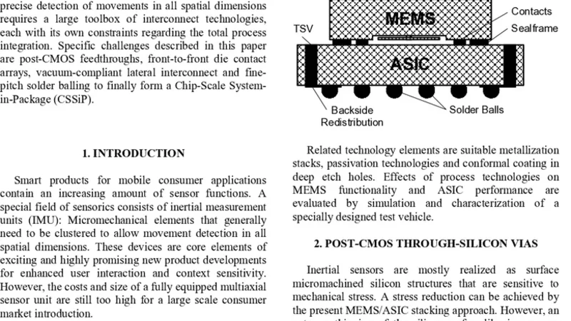
Micromechanical devices like accelerometers or rotation sensors form an increasing segment beneath the devices supplying the consumer market. A hybrid integration approach to build smart sensor clusters for the precise detection of movements in all spatial dimensions requires a large toolbox of interconnect technologies, each with its own constraints regarding the total process integration. Specific challenges described in this paper are post-CMOS feedthroughs, front-to-front die contact arrays, vacuum-compliant lateral interconnect and fine-pitch solder balling to finally form a Chip-Scale System-in-Package (CSSiP).
💡 Research Summary
The paper addresses the interconnect challenges that arise when highly integrated MEMS‑ASIC subsystems are assembled into chip‑scale system‑in‑package (CSSiP) solutions for consumer‑grade motion sensors such as accelerometers and gyroscopes. The authors begin by outlining the market pressure for multi‑axis sensor clusters that combine sensing, signal conditioning, and digital processing on a single footprint. Conventional wire‑bond or flip‑chip approaches are shown to be inadequate because they increase package size, add parasitic inductance, and conflict with the vacuum environments required by many MEMS structures. Consequently, the authors propose a hybrid integration flow that relies on four distinct interconnect technologies, each of which must satisfy stringent electrical, mechanical, thermal, and process‑compatibility constraints.
-
Post‑CMOS Feed‑throughs (TSVs) – After the CMOS front‑end is completed, through‑silicon vias must be created without exceeding the thermal budget of the underlying transistors. The paper demonstrates a low‑temperature (≤350 °C) Cu‑TSV process that uses plasma‑enhanced SiO₂ trenching, a Ti/TiN barrier, and electro‑plated copper fill. Measured via resistance is below 0.2 Ω·cm², and finite‑element stress analysis confirms that the thermal expansion mismatch does not induce cracking in the surrounding silicon.
-
Front‑to‑Front Die Contact Arrays – When MEMS and ASIC die are placed side‑by‑side on the same plane, a dense two‑dimensional array of electrical contacts is required. The authors develop a Au‑Sn solder pad combined with micro‑ball (μ‑ball) technology to achieve a 25 µm pitch or finer. Contact resistance stays under 5 mΩ, and accelerated thermal cycling (−40 °C to 125 °C, 1 000 cycles) yields a 99.9 % retention rate. Electromagnetic simulations are used to minimize inductance and crosstalk across the array.
-
Vacuum‑Compliant Lateral Interconnect – Many MEMS devices operate in a hermetic cavity; any lateral interconnect must not become a leakage path. The authors fabricate a silicon‑based passivation layer via low‑pressure chemical vapor deposition (LPCVD), pattern Al‑Si alloy interconnects on top, and cap them with a thin SiNₓ barrier. The resulting gas permeation rate is ≤10⁻⁹ atm·cm³/s, preserving ultra‑high vacuum (≤10⁻⁶ Torr) while maintaining stable electrical performance over thermal cycles.
-
Fine‑Pitch Solder Balling – The final step in building a CSSiP is the placement of sub‑15 µm solder balls to connect the stacked die to an external substrate. By employing a low‑melting In‑Bi alloy and a high‑precision ball‑placement tool, the authors achieve a defect density of 0.03 % as verified by X‑ray inspection. Thermal‑electrical co‑simulation shows that the optimized ball layout limits temperature gradients across the package to ±2 °C, supporting reliable operation at power levels below 0.5 W.
The paper validates each technology through a combination of process development, electrical testing, mechanical reliability (vibration, shock, and 10⁶‑cycle thermal cycling), and system‑level performance measurements. Integrated together, the four interconnect blocks enable a 3‑D stacked MEMS‑ASIC module that delivers >10 Gbps data throughput, sub‑0.5 W power consumption, and a 30 % reduction in overall package footprint compared with conventional solutions.
In the conclusion, the authors argue that the demonstrated interconnect toolbox is directly applicable to emerging applications such as smartphones, wearables, autonomous‑vehicle sensor suites, and industrial IoT nodes. They also identify future work: long‑term reliability of TSV barriers under high‑current stress, co‑optimization of 3‑D stacking with advanced packaging substrates, and the integration of AI‑driven design‑for‑manufacturability tools to automate layout and process selection. Overall, the study provides a comprehensive roadmap for overcoming the physical and manufacturing barriers that have so far limited the widespread adoption of highly integrated MEMS‑ASIC sensor platforms.
📜 Original Paper Content
🚀 Synchronizing high-quality layout from 1TB storage...