📝 Original Info
- Title: Packaging of RF Mems Switching Functions on Alumina Substrate
- ArXiv ID: 0711.3297
- Date: 2007-11-29
- Authors: Researchers from original ArXiv paper
📝 Abstract
Recently the strong demands in wireless communication requires expanding development for the application of RF MEMS (Radio Frequency micro electro mechanical systems) sensing devices such as micro-switches, tunable capacitors because it offers lower power consumption, lower losses, higher linearity and higher Q factors compared with conventional communications components. To accelerate commercialisation of RF MEMS products, development for packaging technologies is one of the most critical issues should be solved beforehand.
💡 Deep Analysis
Deep Dive into Packaging of RF Mems Switching Functions on Alumina Substrate.
Recently the strong demands in wireless communication requires expanding development for the application of RF MEMS (Radio Frequency micro electro mechanical systems) sensing devices such as micro-switches, tunable capacitors because it offers lower power consumption, lower losses, higher linearity and higher Q factors compared with conventional communications components. To accelerate commercialisation of RF MEMS products, development for packaging technologies is one of the most critical issues should be solved beforehand.
📄 Full Content
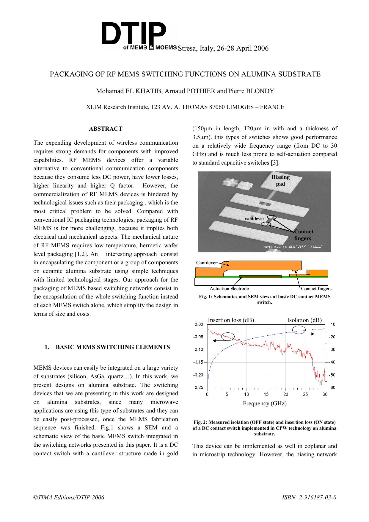
MEMS devices can easily be integrated on a large variety of substrates (silicon, AsGa, quartz…). In this work, we present designs on alumina substrate. The switching devices that we are presenting in this work are designed on alumina substrates, since many microwave applications are using this type of substrates and they can be easily post-processed, once the MEMS fabrication sequence was finished. Fig. 1 shows a SEM and a schematic view of the basic MEMS switch integrated in the switching networks presented in this paper. It is a DC contact switch with a cantilever structure made in gold (150µm in length, 120µm in with and a thickness of 3.5µm). this types of switches shows good performance on a relatively wide frequency range (from DC to 30 GHz) and is much less prone to self-actuation compared to standard capacitive switches [3].
MEMS devices are intented to be packaged in a microcavity fabricated by micromaching of a low cost glass substrate,which is directly bonded on the alumina wafer using gold-to-gold thermo-compression technique, avoiding any biasing or transmision line feedthrough underneath the sealing ring. The glass cap allows MEMS components to be hermetically encapsulated at the wafer scale in a controlled atmosphere. The RF coplanar access will be patterned on the lower alumina substrate side and will be connected to the MEMS active function built on the other subtrate side, through laser drilled full metallized vias holes, These coplanar access will facilitate the packaged component report using flip-chip technics . the via hole process in alumina substrate is now a mature and a very well controlled technology: several companies provide standard alumina substrates already laser drilled with metallized vias. This packaging approach remains compatible with additional circuit fabrication on the same wafer (filters, phase shifters, antennas…) and does not necessarily require individual cap cutting or etching. Fig 3 and4 present side and top views of SPST(Single Port Single Throw) based on a single MEMS switch encapsulated as we described above. The micro-package RF performance depends mainly on the RF transitions used through the substrate. In fact, the RF transition matching could be easily adjusted by optmising the two gap values G1 and G2 between via holes and the CPW ground plane. In fact vias holes present an inductive influence as the frequency increases; the effect of this parasitic inductance on the package performance could be compensated ajusting the capacitance between vias holes and ground plane. The input impedance of the CPW access introduce also an important influence that has been optimized to reach the performances presented on Frequency (GHz) simulated insertion loss is evaluated to be below 0.1dB until 2GHz and 0.7dB up to 30GHz (fig.9.b). This small degradation of the device performance could be explained by a small mismatching at the cross junction. The predicted RF performance in the OFF state seems to be correct until 20 GHz with isolation level better than 15 dB between the regarding RF access. Based on previous results for the basic devices, more complex component can be designed. The SP4T (Single Port Four Throw) example presented on Fig 10, is obtained by combining 3 SPDT devices. The global geometry has been optimized in order to minimize the size of the final structure and improve its performance as much as possible. In this specific topology, two DC contact switches need to be actuated at the same time to allow the signal transmission to any of the four-output access. This series combination will result in an isolation level improvement as shown on Fig. 11. On the other hand, the global transmission loss on each trajectory will increase due to the addition of the actuated individual MEMS switch loss. Consequently, the SP4T have been specifically optimized for instance to obtain the best performance until 20 GHz. At higher frequencies, one can notice the appearance of parasitic modes and degradation of the circuit performance. More work is needed to extend the useful frequency band above this limitation. Yet the SP4T potentially reach insertion loss better than 0.9 dB with return loss level better than of 20 dB from DC up to 20 GHz. In addition, the isolation level between all accesses is always better than 20 dB in the same frequency band.
In this paper is presented an original packaging approach for the development of RF MEMS switching networks on alumina substrate. This approach has the potentiality to be a low cost solution since it stays at the wafer level and it is compatible with the existing alumina processing technology. The developed packaged MEMS functions seem to present very interesting performances on a wide frequency band. We are currently working on the different device fabrication to validate the simulation results. Latest results will be presented during the conference presentation.
📸 Image Gallery
Reference
This content is AI-processed based on ArXiv data.