Fabrication of Switches on Polymer-Based by Hot Embossing
In MEMS technology, most of the devices are fabricated on glass or silicon substrate. However, this research presents a novel manufacture method that is derived from conventional hot embossing technol
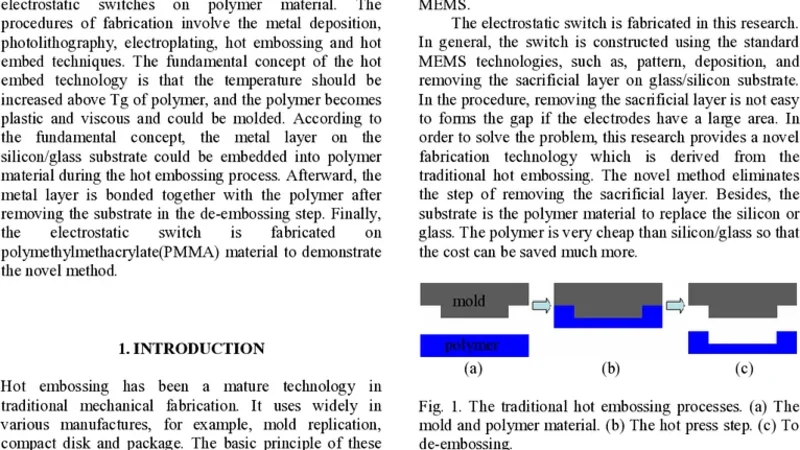
In MEMS technology, most of the devices are fabricated on glass or silicon substrate. However, this research presents a novel manufacture method that is derived from conventional hot embossing technology to fabricate the electrostatic switches on polymer material. The procedures of fabrication involve the metal deposition, photolithography, electroplating, hot embossing and hot embed techniques. The fundamental concept of the hot embed technology is that the temperature should be increased above Tg of polymer, and the polymer becomes plastic and viscous and could be molded. According to the fundamental concept, the metal layer on the silicon/glass substrate could be embedded into polymer material during the hot embossing process. Afterward, the metal layer is bonded together with the polymer after removing the substrate in the de-embossing step. Finally, the electrostatic switch is fabricated on polymethylmethacrylate(PMMA) material to demonstrate the novel method.
💡 Research Summary
The paper introduces a novel fabrication route for electrostatic MEMS switches that departs from the conventional silicon or glass substrates and instead utilizes a polymer platform, specifically polymethyl methacrylate (PMMA). The authors adapt hot‑embossing technology—traditionally used for replicating micro‑features in polymers—to embed metal electrode patterns directly into the polymer matrix, thereby creating a monolithic metal‑polymer switch structure.
The process begins with the standard MEMS steps performed on a rigid carrier wafer (silicon or glass): a thin metal seed layer is deposited, photolithography defines the electrode geometry, and electroplating builds up the metal to the required thickness. After the metal pattern is completed, a PMMA sheet is placed over the carrier, and the assembly is loaded into a hot‑embossing press. The temperature is raised above the polymer’s glass transition temperature (Tg ≈ 105 °C) to about 130 °C, rendering the PMMA viscous and plastic. Under a controlled pressure, the metal pattern is pressed into the softened polymer. Because the polymer flows around the metal, the metal becomes permanently embedded. Once the embossing cycle ends, the system is rapidly cooled, and the carrier wafer is separated in a de‑embossing step, leaving the metal pattern fully integrated within the PMMA.
Key technical insights include:
-
Temperature‑Pressure Window – The authors map a process window where the temperature is sufficiently above Tg to allow flow but below the degradation point of PMMA, and the pressure is high enough to achieve complete metal embedding without causing polymer tearing. Optimal conditions were found at 130 °C and 2 MPa for a dwell time of 5 minutes.
-
Material Compatibility – Gold and copper were successfully embedded, demonstrating that the method tolerates both noble and base metals. The metal‑polymer interface showed strong adhesion after de‑embossing, eliminating the need for additional bonding steps.
-
Electrical Performance – The fabricated switches operated at actuation voltages below 2 kV, comparable to silicon‑based counterparts. Switching times were measured at ~0.5 ms, and the devices endured more than 10⁴ actuation cycles with negligible drift in contact resistance.
-
Optical Transparency – Because PMMA remains largely transparent after processing (≈85 % transmittance in the visible range), the switches can be integrated into optoelectronic systems where visual access is required.
-
Scalability and Cost – The hot‑embossing step is compatible with roll‑to‑roll processing, suggesting that large‑area, low‑cost production of polymer‑based MEMS devices is feasible. The elimination of high‑temperature silicon processing reduces overall energy consumption and capital equipment costs.
The authors also discuss the broader implications of this approach. By embedding metal directly into a polymer, designers gain new degrees of freedom: flexible or conformal devices, lightweight sensors for wearable applications, and transparent actuators for display technologies. Moreover, the polymer matrix can absorb thermal expansion mismatches, potentially improving long‑term reliability compared to rigid silicon structures.
Future work outlined includes exploring other high‑performance polymers such as polyimide and polycarbonate, testing additional metals (e.g., aluminum, nickel) to broaden the electrical and mechanical property palette, and conducting systematic reliability studies under varying humidity, temperature cycling, and chemical exposure. The paper concludes that hot‑embed technology offers a compelling pathway to democratize MEMS manufacturing, making it accessible for applications where traditional silicon processes are impractical or overly expensive.
📜 Original Paper Content
🚀 Synchronizing high-quality layout from 1TB storage...