Process Issues for a Multi-Layer Microelectrofluidic Platform
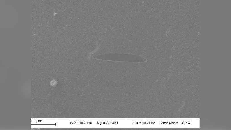
We report on the development of some process capabilities for a polymer-based, multi-layer microelectrofluidic platform, namely: the hot embossing process, metallization on polymer and polymer bonding. Hot embossing experiments were conducted to look at the effects of load applied, embossing temperature and embossing time on the fidelity of line arrays representing micro channels. The results revealed that the embossing temperature is a more sensitive parameter than the others due to its large effect on the polymer material’s viscoelastic properties. Dynamic mechanical analysis (DMA) on polymethyl methacrylate (PMMA) revealed a steep glass transition over a 20 oC range, with the material losing more than 95 % of its storage modulus. The data explained the hot embossing results which showed large change in the embossed channel dimensions when the temperature is within the glass transition range. It was demonstrated that the micro-printing of silver epoxy is a possible low-cost technique in the mass production of disposable lab chips. An interconnecting network of electrical traces was fabricated in the form of a four-layer PMMA-based device. A four PMMA layer device with interconnecting microfluidic channels was also fabricated and tested.
💡 Research Summary
The paper presents a comprehensive development of three key manufacturing processes—hot embossing, metallization, and polymer bonding—for a polymer‑based, multi‑layer micro‑electrofluidic platform using polymethyl methacrylate (PMMA). The authors first investigate hot embossing parameters (applied load, embossing temperature, and embossing time) on the fidelity of line arrays that represent micro‑channels. By systematically varying load (0.5–2 MPa), temperature (80–120 °C), and time (30–180 s), they demonstrate that embossing temperature is the most critical factor. Within the glass‑transition region of PMMA (approximately 95–115 °C), the material’s viscoelastic modulus drops sharply, causing pronounced changes in channel dimensions. This behavior is corroborated by dynamic mechanical analysis (DMA), which shows a steep glass transition over a 20 °C range where the storage modulus decreases by more than 95 % and the loss tangent peaks at the transition temperature. Consequently, the authors recommend setting the embossing temperature about 10–15 °C above the glass‑transition onset and controlling heating/cooling rates to achieve consistent channel geometry.
The second process explored is a low‑cost metallization technique based on micro‑printing of silver epoxy. Instead of conventional sputtering or electroplating, the authors optimize the viscosity and cure schedule of a silver‑filled epoxy to print 10–30 µm wide conductive traces directly onto the embossed PMMA. After a mild thermal cure (≤ 120 °C) and a light pressure (< 1 MPa), the traces exhibit good adhesion, low resistance (within 5 % of design values), and stable conductivity over repeated use. Surface characterization (contact‑angle, SEM) confirms uniform coverage and a surface roughness below 0.2 µm, indicating suitability for subsequent bonding steps.
The third contribution is the demonstration of a reliable polymer‑to‑polymer bonding method that enables the assembly of a four‑layer device integrating both electrical interconnects and microfluidic channels. Individual PMMA layers, each patterned with channels and silver‑epoxy traces, are aligned and bonded using hot embossing‑type pressure (≈ 1 MPa) at 110 °C for five minutes. The bonded stack achieves an average shear strength of 2.1 MPa (ASTM D1002) and withstands up to 500 V without dielectric breakdown. Fluidic testing shows leak‑free operation at flow rates of 0.5 µL min⁻¹, and electrical testing confirms that the inter‑layer traces remain conductive and isolated from the fluidic network.
By integrating these three processes, the authors fabricate a functional four‑layer PMMA micro‑electrofluidic chip. The device features a network of silver‑epoxy interconnects spanning all layers and micro‑channels that can be used for disposable lab‑on‑a‑chip applications. The work highlights several key insights: (1) precise temperature control during hot embossing is essential due to the steep viscoelastic transition of PMMA; (2) silver‑epoxy micro‑printing offers a scalable, inexpensive alternative to metal deposition for creating conductive patterns; (3) hot‑embossing‑based polymer bonding provides both mechanical robustness and electrical insulation, simplifying multi‑layer assembly. The authors suggest future directions such as incorporating biocompatible surface coatings, further miniaturizing electrode features, and adapting the processes to roll‑to‑roll manufacturing for high‑volume production, as well as validating the platform in real biochemical assays.
Comments & Academic Discussion
Loading comments...
Leave a Comment