We present a CAD framework for CMOL, a hybrid CMOS/ molecular circuit architecture. Our framework first transforms any logically synthesized circuit based on AND/OR/NOT gates to a NOR gate circuit, and then maps the NOR gates to CMOL. We encode the CMOL cell assignment problem as boolean conditions. The boolean constraint is satisfiable if and only if there is a way to map all the NOR gates to the CMOL cells. We further investigate various types of static defects for the CMOL architecture, and propose a reconfiguration technique that can deal with these defects through our CAD framework. This is the first automated framework for CMOL cell assignment, and the first to model several different CMOL static defects. Empirical results show that our approach is efficient and scalable.
Deep Dive into Defect-Tolerant CMOL Cell Assignment via Satisfiability.
We present a CAD framework for CMOL, a hybrid CMOS/ molecular circuit architecture. Our framework first transforms any logically synthesized circuit based on AND/OR/NOT gates to a NOR gate circuit, and then maps the NOR gates to CMOL. We encode the CMOL cell assignment problem as boolean conditions. The boolean constraint is satisfiable if and only if there is a way to map all the NOR gates to the CMOL cells. We further investigate various types of static defects for the CMOL architecture, and propose a reconfiguration technique that can deal with these defects through our CAD framework. This is the first automated framework for CMOL cell assignment, and the first to model several different CMOL static defects. Empirical results show that our approach is efficient and scalable.
In recent years, nanoelectronics has made tremendous progress, with advances in novel nanodevices [18], nanocircuits [1,5], nano-crossbar arrays [2,8,12], manufacture by nanoimprint lithography [10,19], CMOS/nano co-design architectures [3,9,20], and applications [15][16][17]. Although a two-terminal nanowire crossbar array does not have the functionality of FET-based circuits, it has the potential for incredible density and low fabrication costs [9]. Likharev and his colleagues [9] have developed the concept of CMOL (Cmos / nanowire / MOLecular hybrid) as a likely implementation technology for charge-based nanoelectronics devices. Examples include memory, FPGA, and neuromorphic CrossNets [15][16][17].
In this paper, we present a framework for CMOL cell assignment. We transform any boolean circuit based on AND/OR/NOT gates to a circuit of NOR gates, and then map the NOR gates to the CMOL architecture. We formulate the CMOL cell mapping task as a set of boolean con-“off” -> “on” “on” state “off” state “on” state “on” -> “off” 0 I V V t Figure 1. Schematic I-V curve of a twoterminal nanodevice (adapted from [9]). ditions, and solve them through satisfiability. Prior work on CMOL [9] was assigning cells by hand. Our technique is the first automated CMOL cell assignment framework. We further investigate various defect models for the CMOL technology, and propose a reconfiguration technique that can deal with all these defects through our cell assignment framework. This is the first detailed study on numerous CMOL defect models.
CMOL was originally developed by Likharev and his colleagues [9]. The nanodevice in CMOL is a binary “latching switch” based on molecules with two metastable internal states. Fig. 1 shows the schematic I-V curve of this twoterminal nanodevice. Qualitatively, if the drain-to-source voltage is low during programming, the nanodevice will be in the “off” state with a high resistance; if the applied voltage is greater than a certian value, the nanodevice will be in the “on” state with a lower resistance. In the operating mode, if the nanodevice is in the “on” state and the applied voltage to the drain and source is greater than the threshold voltage V t , the I-V curve will be like the I-V curve of a finite resistor. If the applied voltage is less than threshold voltage, then the nanodevice is virtually in the “off” state. However, it is not certain yet how large the on-off resistances are and how long the nanodevice can keep its programmed state. From our previous analysis [6], for an aggressive assumption of CMOL’s parameters with 6 nm nanowire pitch, the nanodevice “on” resistance could exhibit a higher value than that of a reasonable length of nanowire (e.g., 6 µm).
To avoid routing the critical signal path via multiple nanodevices is one of the synthesis and routing rules we need to be aware of. In this paper, we address the CMOL cell assignment problem with the understanding that routing between two cells through the nanowire fabric will involve one nanodevice only (see Section 3.2). Fig. 2 shows the basic CMOL circuit, especially the interface between CMOS and nanowires. The pins connect the CMOS upper-level metals and the nanowires. The nanodevices are sandwiched between the two levels of perpendicular nano-imprinted nanowires. This unique structure solves the problems of addressing much denser nanodevices with sparser CMOS components. Each nanodevice is accessed by the two perpendicular nanowires which connect to the nanodevice. The nanowires are in turn connected by the pins which interface with the CMOS circuits. With O(N ) nanowires and pins, we could address O(N 2 ) nanodevices.
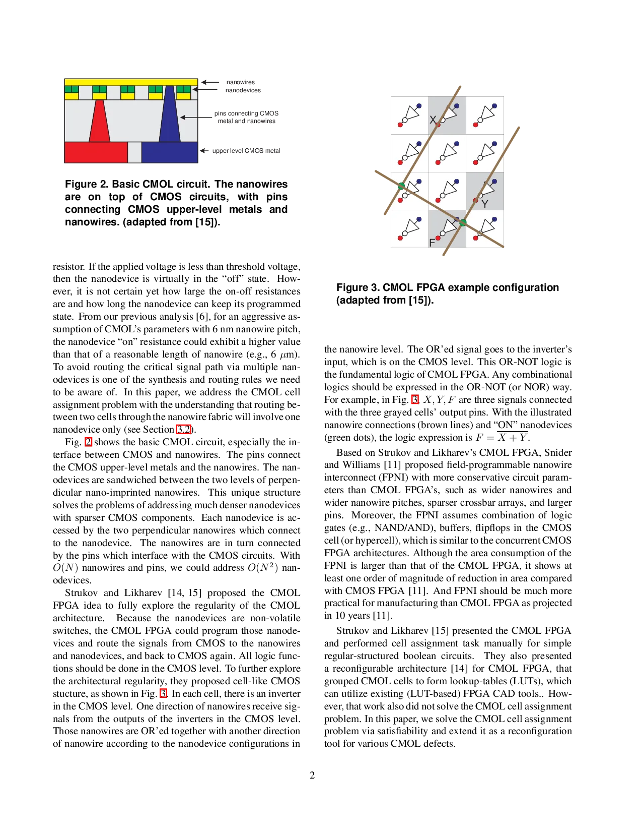
Strukov and Likharev [14,15] proposed the CMOL FPGA idea to fully explore the regularity of the CMOL architecture. Because the nanodevices are non-volatile switches, the CMOL FPGA could program those nanodevices and route the signals from CMOS to the nanowires and nanodevices, and back to CMOS again. All logic functions should be done in the CMOS level. To further explore the architectural regularity, they proposed cell-like CMOS stucture, as shown in Fig. 3. In each cell, there is an inverter in the CMOS level. One direction of nanowires receive signals from the outputs of the inverters in the CMOS level. Those nanowires are OR’ed together with another direction of nanowire according to the nanodevice configurations in the nanowire level. The OR’ed signal goes to the inverter’s input, which is on the CMOS level. This OR-NOT logic is the fundamental logic of CMOL FPGA. Any combinational logics should be expressed in the OR-NOT (or NOR) way. For example, in Fig. 3, X, Y, F are three signals connected with the three grayed cells’ output pins. With the illustrated nanowire connections (brown lines) and “ON” nanodevices (green dots), the logic expression is F = X + Y .
Based on Strukov and Likharev’s CMOL FPGA, Snider and Williams [11] proposed field-programmable nanowire interconnect (FPNI) with more co
…(Full text truncated)…
This content is AI-processed based on ArXiv data.